Showing posts with label photonics. Show all posts

Monday, March 7, 2016

Step towards ‘holy grail’ of silicon photonics


Creation of first practical silicon-based laser has the potential to transform communications, healthcare and energy systems

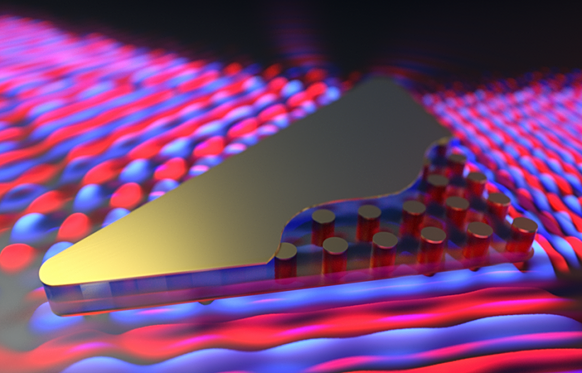
A group of researchers from the UK, including academics from Cardiff University, has demonstrated the first practical laser that has been grown directly on a silicon substrate.

It is believed the breakthrough could lead to ultra-fast communication between computer chips and electronic systems and therefore transform a wide variety of sectors, from communications and healthcare to energy generation.

The EPSRC-funded UK group, led by Cardiff University and including researchers from UCL and the University of Sheffield, have presented their findings in the journal Nature Photonics.

Silicon is the most widely used material for the fabrication of electronic devices and is used to fabricate semiconductors, which are embedded into nearly every device and piece of technology that we use in our everyday lives, from smartphones and computers to satellite communications and GPS.

Electronic devices have continued to get quicker, more efficient and more complex, and have therefore placed an added demand on the underlining technology.

Researchers have found it increasingly difficult to meet these demands using conventional electrical interconnects between computer chips and systems, and have therefore turned to light as a potential ultra-fast connector.

Whilst it has been difficult to combine a semiconductor laser – the ideal source of light – with silicon, the UK group have now overcome these difficulties and successfully integrated a laser directly grown onto a silicon substrate for the very first time.

Professor Huiyun Liu, who led the growth activity, explained that the 1300 nm wavelength laser has been shown to operate at temperatures of up to 120°C and for up to 100,000 hours.

Professor Peter Smowton, from the School of Physics and Astronomy, said: “Realising electrically-pumped lasers based on Si substrates is a fundamental step towards silicon photonics.

“The precise outcomes of such a step are impossible to predict in their entirety, but it will clearly transform computing and the digital economy, revolutionise healthcare through patient monitoring, and provide a step-change in energy efficiency.

“Our breakthrough is perfectly timed as it forms the basis of one of the major strands of activity in Cardiff University’s Institute for Compound Semiconductors and the University’s joint venture with compound semiconductor specialists IQE.”

Professor Alwyn Seeds, Head of the Photonics Group at University College London, said: “The techniques that we have developed permit us to realise the Holy Grail of silicon photonics - an efficient and reliable electrically driven semiconductor laser directly integrated on a silicon substrate. Our future work will be aimed at integrating these lasers with waveguides and drive electronics leading to a comprehensive technology for the integration of photonics with silicon electronics"

Wednesday, January 20, 2016

Watching Electrons Cool in 30 Quadrillionths of a Second


Two University of California, Riverside assistant professors of physics are among a team of researchers that have developed a new way of seeing electrons cool off in an extremely short time period.

The development could have applications in numerous places where heat management is important, including visual displays, next-generation solar cells and photodetectors for optical communications.

In visual displays, such as those used in cell phones and computer monitors, and photodetectors, which have a wide variety of applications including solar energy harvesting and fiber optic telecommunications, much of the energy of the electrons is wasted by heating the material.

Controlling the flow of heat in the electrons, rather than wasting this energy by heating the material, could potentially increase the efficiency of such devices by converting excess energy into useful power.

The research is outlined in a paper, “Tuning ultrafast electron thermalization pathways in a van der Waals heterostructure,” published online Monday (Jan. 18) in the journal Nature Physics. Nathan Gabor and Joshua C.H. Lui, assistant professors of physics at UC Riverside, are among the co-authors.

In electronic materials, such as those used in semiconductors, electrons can be rapidly heated by pulses of light.  The time it takes for electrons to cool each other off is extremely short, typically less than 1 trillionth of a second.

To understand this behavior, researchers use highly specialized tools that utilize ultra-fast laser techniques. In the two-dimensional material graphene cooling excited electrons occurs even faster, taking only 30 quadrillionths of a second. Previous studies struggled to capture this remarkably fast behavior.


To solve that, the researchers used a completely different approach. They combined single layers of graphene with thin layers of insulating boron nitride to form a sandwich structure, known as a van der Waals heterostructure, which gives electrons two paths to choose from when cooling begins. Either the electrons stay in graphene and cool by bouncing off one another, or they get sucked out of graphene and move through the surrounding layer.

By tuning standard experimental knobs, such as voltage and optical pulse energy, the researchers found they can precisely control where the electrons travel and how long they take to cool off. The work provides new ways of seeing electrons cool off at extremely short time scales, and demonstrates novel devices for nanoscale optoelectronics.

This structure is one of the first in a new class of devices that are synthesized by mechanically stacking atomically thin membranes. By carefully choosing the materials that make up the device, the researchers developed a new type of optoelectronic photodetector that is only 10 nanometers thick. Such devices address the technological drive for ultra-dense, low-power, and ultra-efficient devices for integrated circuits.

The research follows advances made in 2011 Science article, in which the research team discovered the fundamental importance of hot electrons in the optoelectronic response of devices based on graphene.

Other co-authors of the Nature Physics paper are: Qiong Ma, Trond I. Andersen, Nityan L. Nair, Andrea F. Young, Wenjing Fang, Jing Kong, Nuh Gedik and Pablo Jarillo-Herrero, all of the Massachusetts Institute of Technology; Mathieu Massicotte and Frank H. L. Koppens, both of The Institute of Photonic Sciences in Spain; and Kenji Watanabe and Takashi Taniguchi, both of the National Institute for Materials Science in Japan.


Tuesday, December 1, 2015

The world's fastest nanoscale photonics switch


International team of researchers from Lomonosov Moscow State University and the Australian National University in Canberra created an ultrafast all-optical switch on silicon nanostructures.

This device may become a platform for future computers and permit to transfer data at an ultrahigh speed. The article with the description of the device was published in Nano Letters journal and highlighted in Nature Materials.

This work belongs to the field of photonics - an optics discipline which appeared in the 1960-s, simultaneously with the invention of lasers. Photonics has the same goals as electronics does, but uses photons--the quanta of light--instead of electrons. The biggest advantage of using photons is the absence of interactions between them. As a consequence, photons address the data transmission problem better than electrons. This property can primarily be used for in computing where IPS (instructions per second) is the main attribute to be maximized. The typical scale of eletronic transistors--the basis of contemporary electronic devices--is less than 100 nanometers, wheres the typical scale of photonic transistors stays on the scale of several micrometers.

Nanostructures that are able to compete with the electronic structures--for example, plasmonic nanoparticles--are characterized by low efficiency and significant losses. Therefore, coming up with a compact photonic switch was a very challenging task.

Three years ago several groups of researchers simultaneously discovered an important effect: they found out that silicon nanoparticles are exhibit strong resonances in the visible spectrum - the so-called magnetic dipole resonances. This type of resonance is characterized by strong localization of light waves on subwavelength scales, inside the nanoparticles. This effect turned out to be interesting to researches, but, according to Maxim Shcherbakov, the first author of the article published in Nano Letters, nobody thought that this discovery could create a basis for development of a compact and very rapid photonic switch.

Nanoparticles were fabricated in the Australian National University by e-beam lithography followed by plasma-phase etching. It was done by Alexander Shorokhov, who served an internship in the University as a part of Presidential scholarship for studying abroad. The samples were brought to Moscow, and all the experimental work was carried out at the Faculty of Physics of Lomonosov Moscow State University, in the Laboratory of Nanophotonics and Metamaterials.

"In our experimental research me and my colleague Polina Vabishchevich from the Faculty used a set of nonlinear optics methods that address femtosecond light-matter, -- explains Maxim Shcherbakov. -- We used our femtosecond laser complex acquired as part of the MSU development program".

Eventually, researches developed a "device": a disc 250 nm in diameter that is capable of switching optical pulses at femtosecond rates (femtosecond is a one millionth of one billionth of a second). Switching speeds that fast will allow to create data transmission and processing devices that will work at tens and hundreds terabits per second. This can make possible downloading thousands of HD-movies in less than a second.

The operation of the all-optical switch created by MSU researchers is based on the interaction between two femtosecond pulses. The interaction becomes possible due to the magnetic resonance of the silicon nanostructures. If the pulses arrive at the nanostructure simultaneously, one of them interacts with the other and dampers it due to the effect of two-photon absorption. If there is a 100-fs delay between the two pulses, the interaction does not occur, and the second pulse goes through the nanostructure without changing.

"We were able to develop a structure with the undesirable free-carrier effects are suppressed, -- says Maxim Shcherbakov. -- Free carriers (electrons and electron holes) place serious restrictions on the speed of signal conversion in the traditional integrated photonics. Our work represents an important step towards novel and efficient active photonic devices-- transistors, logic units, and others. Features of the technology implemented in our work will allow its use in silicon photonics. In the nearest future, we are going to test such nanoparticles in integrated circuits".

http://www.nanotechnologyworld.org/#!The-worlds-fastest-nanoscale-photonics-switch/c89r/565dba120cf2c000e929c875 

Monday, November 2, 2015

Record-setting flexible phototransistor

Developed by UW electrical engineers, this unique phototransistor is flexible, yet faster and more responsive than any similar phototransistor in the world. Photo: Jung-Hun Seo


Inspired by mammals' eyes, University of Wisconsin-Madison electrical engineers have created the fastest, most responsive flexible silicon phototransistor ever made.

The innovative phototransistor could improve the performance of myriad products — ranging from digital cameras, night-vision goggles and smoke detectors to surveillance systems and satellites — that rely on electronic light sensors. Integrated into a digital camera lens, for example, it could reduce bulkiness and boost both the acquisition speed and quality of video or still photos.

Developed by UW-Madison collaborators Zhenqiang "Jack" Ma, professor of electrical and computer engineering, and research scientist Jung-Hun Seo, the high-performance phototransistor far and away exceeds all previous flexible phototransistor parameters, including sensitivity and response time.

The researchers published details of their advance this week in the journal Advanced Optical Materials.

Like human eyes, phototransistors essentially sense and collect light, then convert that light into an electrical charge proportional to its intensity and wavelength. In the case of our eyes, the electrical impulses transmit the image to the brain. In a digital camera, that electrical charge becomes the long string of 1s and 0s that create the digital image.

While many phototransistors are fabricated on rigid surfaces, and therefore are flat, Ma and Seo's are flexible, meaning they more easily mimic the behavior of mammalian eyes.

"We actually can make the curve any shape we like to fit the optical system," Ma says. "Currently, there's no easy way to do that."

One important aspect of the success of the new phototransistors is the researchers' innovative "flip-transfer" fabrication method, in which their final step is to invert the finished phototransistor onto a plastic substrate. At that point, a reflective metal layer is on the bottom.

"In this structure — unlike other photodetectors — light absorption in an ultrathin silicon layer can be much more efficient because light is not blocked by any metal layers or other materials," Ma says.

While many phototransistors are fabricated on rigid surfaces, and therefore are flat, Ma and Seo's are flexible, meaning they more easily mimic the behavior of mammalian eyes.

The researchers also placed electrodes under the phototransistor's ultrathin silicon nanomembrane layer — and the metal layer and electrodes each act as reflectors and improve light absorption without the need for an external amplifier.

"There's a built-in capability to sense weak light," Ma says.

Ultimately, the new phototransistors open the door of possibility, he says.

"This demonstration shows great potential in high-performance and flexible photodetection systems," says Ma, whose work was supported by the U.S. Air Force. "It shows the capabilities of high-sensitivity photodetection and stable performance under bending conditions, which have never been achieved at the same time."

Monday, October 19, 2015

To infinity and beyond: Light goes infinitely fast with new on-chip material


Electrons are so 20th century. In the 21st century, photonic devices, which use light to transport large amounts of information quickly, will enhance or even replace the electronic devices that are ubiquitous in our lives today. But there’s a step needed before optical connections can be integrated into telecommunications systems and computers: researchers need to make it easier to manipulate light at the nanoscale.  

Researchers at the Harvard John A. Paulson School of Engineering and Applied Sciences (SEAS) have done just that, designing the first on-chip metamaterial with a refractive index of zero, meaning that the phase of light can travel infinitely fast. 

This new metamaterial was developed in the lab of Eric Mazur, the Balkanski Professor of Physics and Applied Physics and Area Dean for Applied Physics at SEAS, and is described in the journal Nature Photonics.

“Light doesn’t typically like to be squeezed or manipulated but this metamaterial permits you to manipulate light from one chip to another, to squeeze, bend, twist and reduce diameter of a beam from the macroscale to the nanoscale,” said Mazur. “It’s a remarkable new way to manipulate light.”

Although this infinitely high velocity sounds like it breaks the rule of relativity, it doesn’t. Nothing in the universe travels faster than light carrying information — Einstein is still right about that. But light has another speed, measured by how fast the crests of a wavelength move, known as phase velocity. This speed of light increases or decreases depending on the material it’s moving through.

When light passes through water, for example, its phase velocity is reduced as its wavelengths get squished together. Once it exits the water, its phase velocity increases again as its wavelength elongates. How much the crests of a light wave slow down in a material is expressed as a ratio called the refraction index — the higher the index, the more the material interferes with the propagation of the wave crests of light. Water, for example, has a refraction index of about 1.3.

When the refraction index is reduced to zero, really weird and interesting things start to happen.
In a zero-index material, there is no phase advance, meaning light no longer behaves as a moving wave, traveling through space in a series of crests and troughs. Instead, the zero-index material creates a constant phase — all crests or all troughs — stretching out in infinitely long wavelengths.  The crests and troughs oscillate only as a variable of time, not space.

This uniform phase allows the light to be stretched or squished, twisted or turned, without losing energy. A zero-index material that fits on a chip could have exciting applications, especially in the world of quantum computing.  

“Integrated photonic circuits are hampered by weak and inefficient optical energy confinement in standard silicon waveguides,” said Yang Li, a postdoctoral fellow in the Mazur Group and first author on the paper. “This zero-index metamaterial offers a solution for the confinement of electromagnetic energy in different waveguide configurations because its high internal phase velocity produces full transmission, regardless of how the material is configured.” 

The metamaterial consists of silicon pillar arrays embedded in a polymer matrix and clad in gold film. It can couple to silicon waveguides to interface with standard integrated photonic components and chips.

“In quantum optics, the lack of phase advance would allow quantum emitters in a zero-index cavity or waveguide to emit photons which are always in phase with one another,” said Philip Munoz, a graduate student in the Mazur lab and co-author on the paper.  “It could also improve entanglement between quantum bits, as incoming waves of light are effectively spread out and infinitely long, enabling even distant particles to be entangled.”

“This on-chip metamaterial opens the door to exploring the physics of zero index and its applications in integrated optics,” said Mazur. 

Tuesday, September 15, 2015

Tracking slow nanolight in natural hyperbolic metamaterial slabs

Tracking slow nanolight in natural hyperbolic metamaterial slabs
Researchers at CIC nanoGUNE (Basque Country) in collaboration with colleagues at ICFO - The Institute of Photonic Sciences (Catalunya) have imaged how light moves inside an exotic class of matter known as hyperbolic materials. They observed, for the first time, ultraslow pulse propagation and backward propagating waves in deep subwavelength-scale thick slabs of boron nitride - a natural hyperbolic material for infrared light. This work has been funded by the EC Graphene Flagship and was recently reported in Nature Photonics.
Hyperbolic materials are very special because they behave like a metal in one direction, but like an insulator in the other. Until now, these materials have been used to fabricate complex nanostructures that permit subwavelength-scale imaging, as well as the focusing and controlling of light at the nanoscale. However, in order to fully exploit their potential, it is necessary to study and understand how light behaves inside them.
The work lays the foundations for studying the precise manner in which light travels through complex optical systems at the subwavelength scale in extremely high levels of detail. Such a capability will be vital for verifying that future nanophotonic devices, perhaps with biosensing or optical computing applications, are functioning as expected.
“The difficulty in performing the reported experiments is the extremely short wavelength of light when it is inside a hyperbolic material” explains Ikerbasque Professor Rainer Hillenbrand, leader of the nanooptics group at nanoGUNE. When light moves inside the material - in our case mid-infrared light in a 135 nm boron nitride slab - it travels in the form of what we call a polariton, where the light is actually coupled to the vibrations of the matter itself".

Thursday, September 10, 2015

How to spawn an “exceptional ring”

A schematic drawing of how a ring of exceptional points (shown in white) can be spawned from a Dirac point (a dot), and thus change the dispersion from the normal, widely known conical shape into an exotic lantern-like shape
Courtesy of the researchers

Researchers create exotic states that could lead to new kinds of sensors and optical devices.


The Dirac cone, named after British physicist Paul Dirac, started as a concept in particle and high-energy physics and has recently became important in research in condensed matter physics and material science. It has since been found to describe aspects of graphene, a two dimensional form of carbon, suggesting the possibility of applications across various fields.
Now physicists at MIT have found another unusual phenomenon produced by the Dirac cone: It can spawn a phenomenon described as a “ring of exceptional points.” This connects two fields of research in physics and may have applications in building powerful lasers, precise optical sensors, and other devices.
The results are published this week in the journal Nature by MIT postdoc Bo Zhen, Yale University postdoc Chia Wei Hsu, MIT physics professors Marin Soljačić and John Joannopoulos, and five others.
This work represents “the first experimental demonstration of a ring of exceptional points,” Zhen says, and is the first study that relates research in exceptional points with the physical concepts of parity-time symmetry and Dirac cones.
Individual exceptional points are a peculiar phenomenon unique to an unusual class of physical systems that can lead to counterintuitive phenomena. For example, around these points, opaque materials may seem more transparent, and light may be transmitted only in one direction. However, the practical usefulness of these properties is limited by absorption loss introduced in the materials.
A schematic picture showing the conical dispersion of a Dirac cone being deformed into a new hour-glass-like shape due to radiation. Courtesy of the researchers
The MIT team used a nanoengineered material called a photonic crystal to produce the exceptional ring. This new ring of exceptional points is different from those studied by other groups, making it potentially more practical, the researchers say.

“Instead of absorption loss, we adopt a different loss mechanism — radiation loss — which does not affect the device performance,” Zhen says. “In fact, radiation loss is useful and is necessary in devices like lasers.”
This phenomenon could enable creation of new kinds of optical systems with novel features, the MIT team says.
“One important possible application of this work is in creating a more powerful laser system than existing technologies allow,” Soljačić says. To build a more powerful laser requires a bigger lasing area, but that introduces more unwanted “modes” for light, which compete for power, limiting the final output.
“Photonic crystal surface-emitting lasers are a very promising candidate for the next generation of high-quality, high-power compact laser systems,” Soljačić says, “and we estimate we can improve the output power limit of such lasers by a factor of at least 10.”
“Our system could also be used for high-precision detectors for biological or chemical materials, because of its extreme sensitivity,” Hsu says. This improved sensitivity is due to another exotic property of the exceptional points: Their response to perturbations is not linear to the perturbation strength.
Normally, Hsu says, it becomes very difficult to detect a substance when its concentration is low. When the concentration of the target substance is reduced by a million times, the overall signal also decreases by a million times, which can make it too small to detect.
“But at an exceptional point, it’s not linear anymore,” Hsu says, “and the signal goes down by only 1,000 times, providing a much bigger response that can now be detected.”
Demetrios Christodoulides, a professor of optics and photonics at the University of Central Florida who was not involved in this work, says, “This represents the first observation of an exceptional ring in a 2-D crystal associated with a two-dimensional band. The MIT work opens up a number of opportunities … in particular, around exceptional points where systems are known on many occasions to behave in a peculiar fashion.”
The research team also included Yuichi Igarashi of NEC Corp. in Japan and MIT research scientist Ling Lu, postdoc Ido Kaminer, Harvard University graduate student Adi Pick, and Song-Liang Chua at DSO National Laboratory in Singapore. The work was supported, in part, by the Army Research Office through MIT’s Institute for Soldier Nanotechnologies, the National Science Foundation, and the Department of Energy.