Showing posts with label Solar Cells. Show all posts

Thursday, October 15, 2015

Quantum physics meets genetic engineering


Nature has had billions of years to perfect photosynthesis, which directly or indirectly supports virtually all life on Earth. In that time, the process has achieved almost 100 percent efficiency in transporting the energy of sunlight from receptors to reaction centers where it can be harnessed — a performance vastly better than even the best solar cells.

One way plants achieve this efficiency is by making use of the exotic effects of quantum mechanics — effects sometimes known as “quantum weirdness.” These effects, which include the ability of a particle to exist in more than one place at a time, have now been used by engineers at MIT to achieve a significant efficiency boost in a light-harvesting system.

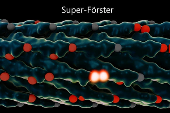
Surprisingly, the MIT researchers achieved this new approach to solar energy not with high-tech materials or microchips — but by using genetically engineered viruses.

This achievement in coupling quantum research and genetic manipulation, described this week in the journal Nature Materials, was the work of MIT professors Angela Belcher, an expert on engineering viruses to carry out energy-related tasks, and Seth Lloyd, an expert on quantum theory and its potential applications; research associate Heechul Park; and 14 collaborators at MIT and in Italy.

Lloyd, a professor of mechanical engineering, explains that in photosynthesis, a photon hits a receptor called a chromophore, which in turn produces an exciton — a quantum particle of energy. This exciton jumps from one chromophore to another until it reaches a reaction center, where that energy is harnessed to build the molecules that support life.

But the hopping pathway is random and inefficient unless it takes advantage of quantum effects that allow it, in effect, to take multiple pathways at once and select the best ones, behaving more like a wave than a particle.


This efficient movement of excitons has one key requirement: The chromophores have to be arranged just right, with exactly the right amount of space between them. This, Lloyd explains, is known as the “Quantum Goldilocks Effect.”

That’s where the virus comes in. By engineering a virus that Belcher has worked with for years, the team was able to get it to bond with multiple synthetic chromophores — or, in this case, organic dyes. The researchers were then able to produce many varieties of the virus, with slightly different spacings between those synthetic chromophores, and select the ones that performed best.

In the end, they were able to more than double excitons’ speed, increasing the distance they traveled before dissipating — a significant improvement in the efficiency of the process.

The project started from a chance meeting at a conference in Italy. Lloyd and Belcher, a professor of biological engineering, were reporting on different projects they had worked on, and began discussing the possibility of a project encompassing their very different expertise. Lloyd, whose work is mostly theoretical, pointed out that the viruses Belcher works with have the right length scales to potentially support quantum effects.

In 2008, Lloyd had published a paper demonstrating that photosynthetic organisms transmit light energy efficiently because of these quantum effects. When he saw Belcher’s report on her work with engineered viruses, he wondered if that might provide a way to artificially induce a similar effect, in an effort to approach nature’s efficiency.

“I had been talking about potential systems you could use to demonstrate this effect, and Angela said, ‘We’re already making those,’” Lloyd recalls. Eventually, after much analysis, “We came up with design principles to redesign how the virus is capturing light, and get it to this quantum regime.”

Within two weeks, Belcher’s team had created their first test version of the engineered virus. Many months of work then went into perfecting the receptors and the spacings.

Once the team engineered the viruses, they were able to use laser spectroscopy and dynamical modeling to watch the light-harvesting process in action, and to demonstrate that the new viruses were indeed making use of quantum coherence to enhance the transport of excitons.

“It was really fun,” Belcher says. “A group of us who spoke different [scientific] languages worked closely together, to both make this class of organisms, and analyze the data. That’s why I’m so excited by this.”

While this initial result is essentially a proof of concept rather than a practical system, it points the way toward an approach that could lead to inexpensive and efficient solar cells or light-driven catalysis, the team says. So far, the engineered viruses collect and transport energy from incoming light, but do not yet harness it to produce power (as in solar cells) or molecules (as in photosynthesis). But this could be done by adding a reaction center, where such processing takes place, to the end of the virus where the excitons end up.

“This is exciting and high-quality research,” says Alán Aspuru-Guzik, a professor of chemistry and chemical biology at Harvard University who was not involved in this work. The research, he says, “combines the work of a leader in theory (Lloyd) and a leader in experiment (Belcher) in a truly multidisciplinary and exciting combination that spans biology to physics to potentially, future technology.”

“​Access to controllable excitonic systems is a goal shared by many researchers in the field,” Aspuru-Guzik adds. “This work provides fundamental understanding that can allow for the development of devices with an increased control of exciton flow.”

The research was supported by the Italian energy company Eni through the MIT Energy Initiative. In addition to MIT postdocs Nimrod Heldman and Patrick Rebentrost, the team included researchers at the University of Florence, the University of Perugia, and Eni.

Monday, April 7, 2014

Organic Solar Cells More Efficient With Molecules Face-to-Face

Molecules in face-on orientation inside
organic solar cell. 
Artist: Peter Allen.
New research from North Carolina State University and UNC-Chapel Hill reveals that energy is transferred more efficiently inside of complex, three-dimensional organic solar cells when the donor molecules align face-on, rather than edge-on, relative to the acceptor. This finding may aid in the design and manufacture of more efficient and economically viable organic solar cell technology.
Organic solar cell efficiency depends upon the ease with which an exciton – the energy particle created when light is absorbed by the material – can find the interface between the donor and acceptor molecules within the cell. At the interface, the exciton is converted into charges that travel to the electrodes, creating power. While this sounds straightforward enough, the reality is that molecules within the donor and acceptor layers can mix, cluster into domains, or both, leading to variances in domain purity and size which can affect the power conversion process. Moreover, the donor and acceptor molecules have different shapes, and the way they are oriented relative to one another matters. This complexity makes it very difficult to measure the important characteristics of their structure.
NC State physicist Harald Ade, UNC-Chapel Hill chemist Wei You and collaborators from both institutions studied the molecular composition of solar cells in order to determine what aspects of the structures have the most impact on efficiency. In this project the team used advanced soft X-ray techniques to describe the orientation of molecules within the donor and acceptor materials. By manipulating this orientation in different solar cell polymers, they were able to show that a face-on alignment between donor and acceptor was much more efficient in generating power than an edge-on alignment.
“A face-on orientation is thought to allow favorable interactions for charge transfer and inhibit recombination, or charge loss, in organic solar cells,” Ade says, “though precisely what happens on the molecular level is still unclear.
“Donor and acceptor layers don’t just lie flat against each other,” Ade explains. “There’s a lot of mixing going on at the molecular level. Picture a bowl of flat pasta, like fettucine, as the donor polymer, and then add ‘ground meat,’ or a round acceptor molecule, and stir it all together. That’s your solar cell. What we want to measure, and what matters in terms of efficiency, is whether the flat part of the fettuccine hugs the round pieces of meat – a face-on orientation – or if the fettuccine is more randomly oriented, or worst case, only the narrow edges of stacked up pasta touch the meat in an edge-on orientation. It’s a complicated problem.
“This research gives us a method for measuring this molecular orientation, and will allow us to find out what the effects of orientation are and how orientation can be fine-tuned or controlled.”
The paper appears online April 6 in Nature Photonics. Fellow NC State collaborators were John Tumbleston, Brian Collins, Eliot Gann, and Wei Ma. Liqiang Yang and Andrew Stuart from UNC-Chapel Hill also contributed to the work. The work was funded by the U.S. Department of Energy, Office of Science, Basic Energy Science, the Office of Naval Research, and the National Science Foundation.
-peake-
 Note to editors: Abstract of the paper follows.
“The influence of molecular orientation on organic bulk heterojunction solar cells”
Authors: John R. Tumbleston, Brian A. Collins, Eliot Gann, Wei Ma and Harald Ade, North Carolina State University; Liqiang Yang, Andrew C. Stuart and Wei You, University of North Carolina at Chapel Hill
Published: April 6, 2014, in Nature Photonics
Abstract:
In bulk heterojunction organic photovoltaics, electron-donating and electron-accepting materials form a distributed network of heterointerfaces in the photoactive layer, where critical photo-physical processes occur. However, little is known about the structural properties of these interfaces due to their complex three-dimensional arrangement and the lack of techniques to measure local order. Here, we report that molecular orientation relative to donor/acceptor heterojunctions is an important parameter in realizing high-performance fullerene-based, bulk heterojunction solar cells. Using resonant soft X-ray scattering, we characterize the degree of molecular orientation, an order parameter that describes face-on (+1) or edge-on (-1) orientations relative to these heterointerfaces. By manipulating the degree of molecular orientation through the choice of molecular chemistry and the characteristics of the processing solvent, we are able to show the importance of this structural parameter on the performance of bulk heterojunction organic photovoltaic devices featuring the electron-donating polymers PNDT–DTBT, PBnDT–DTBT or PBnDT–TAZ.
http://news.ncsu.edu/releases/tp-adephotonics/

Wednesday, January 22, 2014

From a carpet of nanorods to a thin film solar cell absorber within a few seconds

The transformation from a layer of closely packed nanorods
(top left) to a polycrystalline semiconductor thin film (top right)
can be observed in by in-situ X-ray diffraction in real time.
The intensities of the diffraction signals are color coded in the
image at the bottom. A detailed analysis of the signals reveals
that the transformation of the nanorods into kesterite crystals
takes only 9 to 18 seconds.
Picture: R. Mainz/A. Singh
Research teams at the HZB and at the University of Limerick, Ireland, have discovered a novel solid state reaction which lets kesterite grains grow within a few seconds and at relatively low temperatures. For this reaction they exploit a transition from a metastable wurtzite compound in the form of nanorods to the more stable kesterite compound. 
At the EDDI Beamline at BESSY II, the scientists could observe this process in real-time when heating the sample: in a few seconds Kesterite grains formed. The size of the grains was found to depend on the heating rate. With fast heating they succeeded in producing a Kesterite thin film with near micrometer-sized crystal grains, which could be used in thin film solar cells. These findings have now been published in the journal “Nature Communications”.

Grain formation during growth of kesterite solar cells observed in real-time

As starting material for the formation of the kesterite film serves a “carpet of nanorods”: With the help of solution-based chemical processing, the chemists around Ajay Singh and Kevin Ryan at the University of Limerick have fabricated films of highly ordered wurtzite nanorods, which have exactly the same composition as kesterite Cu2ZnSnS4. With the help of real-time X-ray diffraction at the EDDI beamline of BESSY II, HZB physicists around Roland Mainz and Thomas Unold could now observe how a phase transition from the metastable wurtzite phase to the stable kesterite phase leads to a rapid formation of a thin film with large kesterite grains. “It is interesting to see that the complete formation of the kesterite film is so fast”, says Mainz. And the faster the samples are heated up, the larger the grains grow. Mainz explains that at low heating rate, the transition from wurtzite to kesterite starts at lower temperature at which many small grains form – instead of a few larger grains. Additionally, more defects are formed at lower temperatures. During fast heating, the transition takes place at higher temperature at which grains with less defects form.
Moreover, the comparison of the time-resolved evolution of the phase transition during slow and during fast heating shows that not only the grain growth is triggered by the phase transition, but also the phase transition is additionally accelerated by the grain growth. The HZB physicists have developed a model which can explain these findings. By means of numerical model calculations, they demonstrated the accordance of the model with the measured data.
Novel synthesis pathway for thin film semiconductors with controlled morphology
The work points towards a new pathway for the fabrication of thin microcrystalline semiconductor films without the need of expensive vacuum technology. Cu2ZnSnS4-based kesterite semiconductors have gained increasing attention in the past, since they are a promising alternative for the Cu(In,Ga)Se2chalcopyrite solar cells which already achieved efficiencies above 20%. Kesterite has similar physical properties as the chalcopyrite semiconductors, but consist only of elements which are abundantly present in the earth crust. The new procedure could also be interesting for the fabrication of micro- and nanostructured photoelectric devices as well as for semiconductor layers consisting of other materials, says Mainz. “But we continue to focus on kesterites, because this is a really exciting topic at the moment.”
Source: http://www.helmholtz-berlin.de/pubbin/news_seite?nid=13909;sprache=en;typoid=3228

Thursday, December 12, 2013

Quantum waves at the heart of organic solar cells


Researchers have been able to tune ‘coherence’ in organic nanostructures due to the surprise discovery of wavelike electrons in organic materials, revealing the key to generating “long-lived charges” in organic solar cells - material that could revolutionise solar energy.

One does not expect to see such effects in organic molecules - which [...] tend to resemble a plate of cooked spaghettiSimon Gélinas

By using an ultrafast camera, scientists say they have observed the very first instants following the absorption of light into artificial yet organic nanostructures and found that charges not only formed rapidly but also separated very quickly over long distances - phenomena that occur due to the wavelike nature of electrons which are governed by fundamental laws of quantum mechanics.

This result surprised scientists as such phenomena were believed to be limited to "perfect" - and expensive - inorganic structures; rather than the soft, flexible organic material believed by many to be the key to cheap, 'roll-to-roll' solar cells that could be printed at room temperatures - a very different world from the traditional but costly processing of current silicon technologies.

The study, published today in the journal Science, sheds new light on the mystery mechanism that allows positive and negative charges to be separated efficiently - a critical question that continues to puzzle scientists - and takes researchers a step closer to effectively mimicking the highly efficient ability to harvest sunlight and convert into energy, namely photosynthesis, which the natural world evolved over the course of millennia.

"This is a very surprising result. Such quantum phenomena are usually confined to perfect crystals of inorganic semiconductors, and one does not expect to see such effects in organic molecules - which are very disordered and tend to resemble a plate of cooked spaghetti rather than a crystal," said Dr Simon Gélinas, from Cambridge's Cavendish Laboratory, who led the research with colleagues from Cambridge as well as the University of California in Santa Barbara.

During the first few femtoseconds (one millionth of one billionth of a second) each charge spreads itself over multiple molecules rather than being localised to a single one. This phenomenon, known as spatial coherence, allows a charge to travel very quickly over several nanometres and escape from its oppositely charged partner - an initial step which seems to be the key to generating long-lived charges, say the researchers. This can then be used to generate electricity or for chemical reactions.

By carefully engineering the way molecules pack together, the team found that it was possible to tune the spatial coherence and to amplify - or reduce - this long-range separation. "Perhaps most importantly the results suggest that because the process is so fast it is also energy efficient, which could result in more energy out of the solar cell," said Dr Akshay Rao, a co-author on the study from the Cavendish Laboratory.

Dr Alex Chin, who led the theoretical part of the project, added that, if you look beyond the implications of the study for organic solar cells, this is a clear demonstration of "how fundamental quantum-mechanical processes, such as coherence, play a crucial role in disordered organic and biological systems and can be harnessed in new quantum technologies".

The work at Cambridge forms part of a broader initiative to harness high tech knowledge in the physics sciences to tackle global challenges such as climate change and renewable energy. This initiative is backed by both the UK Engineering and Physical Sciences Research Council (EPSRC) and the Cambridge Winton Programme for the Physics of Sustainability. The work at the University of California in Santa Barbara was supported by the Center for Energy Efficient Materials, an Energy Frontier Research Center funded by the U.S. Department of Energy, Office of Science, Basic Energy Sciences under Award #DC0001009.

Source: http://www.cam.ac.uk/research/news/quantum-waves-at-the-heart-of-organic-solar-cells#sthash.bqP9H7Od.dpuf

Thursday, December 5, 2013

Characterizing Solar Cells with Nanoscale Precision Using a Low-Energy Electron Beam

Electron beam induced current (red) superimposed on a scanning 
electron micrograph (gray). Bright contrast in the vicinity of 
grain boundaries indicates that these regions have higher 
carrier collection efficiency than the grain interiors The use 
of electron beam induced current to visualize the behavior of 
photovoltaic cells at these length scales provides a valuable 
tool for understanding both loss mechanisms within photovoltaic 
materials as well as internal structures within these materials 
that may lead to higher overall cell efficiencies.

Researchers from  the NIST Center for Nanoscale Science and Technology (CNST) have demonstrated a new low energy electron beam technique and used it to probe the nanoscale electronic properties of grain boundaries and grain interiors in cadmium telluride (CdTe) solar cells.  Their results suggest that controlling material properties near the grain boundaries could provide a path for increasing the efficiency of such solar cells.
Among thin film photovoltaic solar cells, those made from cadmium telluride are some of the most successful on the market.  However, the efficiency of commercial cells is still less than half of the theoretical maximum, and the underlying mechanisms for the deficiency are not well understood.  CdTe cells are believed to lose current at their material grain boundaries; however, it has also been suggested these grain boundaries have properties that could actually improve carrier collection if they were better understood.  
Characterization techniques using focused electron beams to induce currents are increasingly used for investigating the properties of thin film solar cells.  The measurements are easier using high energy electrons, but the higher energy reduces the spatial resolution.  The researchers extended traditional electron-beam-induced current measurements by using low energy beams to locally excite the CdTe and create current.  These beams have a spatial resolution of about 20 nm, small enough to map the photocurrent response inside the grain interiors or at the grain boundaries.
The measurements were performed on fragments extracted from a commercial thin film solar cell.  Nanoscale electrical contacts were prepared with sizes comparable to a single or a few grains, confining the current path to sizes relevant for understanding current production and loss.  
The measurements show that a large fraction of grain boundaries display higher current collection than the grain interiors, seemingly enhancing device performance.  However, using 2D finite element simulations, the researchers demonstrated that these grain boundaries also create a large pathway for leakage current, which completely negates the efficiency gains from the enhanced photocurrent collection.  
The researchers believe that their technique provides a valuable tool for visualizing the behavior of photovoltaic cells at the length scales needed to understand both loss mechanisms within photovoltaic materials as well as internal structures within these materials that may lead to higher overall cell efficiencies.  
*Local electrical characterization of cadmium telluride solar cells using  low-energy electron beam, H. P. Yoon, P. M. Haney, D. Ruzmetov, H. Xu,  M. S. Leite, B. H. Hamadani, A. A. Talin, and N. B. Zhitenev, Solar Energy Materials and Solar Cells 117, 499-504 (2013).

Saturday, October 26, 2013

How to move photovoltaic solar cell technology toward record-breaking efficiencies?

The atomic arrangement at a relaxed InGaN/GaN interface
The atomic arrangement at a relaxed InGaN/GaN interface. Research at ASU and Georgia Tech show layer-by-layer crystal growth may lead to record-breaking efficiencies in photovoltaic solar cell technology.
Photo by: Arizona State University
Crystals are at the heart of diodes. Not the kind you might find in quartz, formed naturally, but manufactured to form alloys, such as indium gallium nitride or InGaN. 
This alloy forms the light emitting region of LEDs, for illumination in the visible range, and of laser diodes (LDs), in the blue-UV range. Did you know that crystals form the basis for the penetrating icy blue glare of car headlights and could be fundamental to the future in solar energy technology?
Research into making better crystals with high crystalline quality, light emission efficiency and luminosity is also at the heart of studies being done at Arizona State University by research scientist Alec Fischer and doctoral candidate Yong Wei in professor Fernando Ponce’s group in the Department of Physics.
In an article recently published in the journal Applied Physics Letters, the ASU group, in collaboration with a scientific team led by professor Alan Doolittle at the Georgia Institute of Technology, has just revealed the fundamental aspect of a new approach to growing InGaN crystals for diodes, which promises to move photovoltaic solar cell technology toward record-breaking efficiencies.
Solar energy crystallizes
The InGaN crystals are grown as layers in a sandwich-like arrangement on sapphire substrates. Typically, researchers have found that the atomic separation of the layers varies; a condition that can lead to high levels of strain, breakdowns in growth and fluctuations in the alloy’s chemical composition.
“Being able to ease the strain and increase the uniformity in the composition of InGaN is very desirable,” says Ponce, “but difficult to achieve. Growth of these layers is similar to trying to smoothly fit together two honeycombs with different cell sizes, where size difference disrupts a periodic arrangement of the cells.”
As outlined in their publication, the authors developed an approach where pulses of molecules were introduced to achieve the desired alloy composition. The method, developed by Doolittle, is called metal-modulated epitaxy. “This technique allows an atomic, layer-by-layer growth of the material,” says Ponce. 
Analysis of the atomic arrangement and the luminosity at the nanoscale level was performed by Fischer, the lead author of the study, and Wei. Their results showed that the films grown with the epitaxy technique had almost ideal characteristics and revealed that the unexpected results came from the strain relaxation at the first atomic layer of crystal growth.

“Doolittle’s group was able to assemble a final crystal that is more uniform and whose lattice structures match up … resulting in a film that resembles a perfect crystal,” says Ponce. “The luminosity was also like that of a perfect crystal. Something that no one in our field thought was possible.”
The perfect solar cell?
The ASU and Georgia Tech team’s elimination of these two seemingly insurmountable defects (non-uniform composition and mismatched lattice alignment) ultimately means that LEDs and solar photovoltaic products can now be developed that have much higher, efficient performance.
“While we are still a ways off from record-setting solar cells, this breakthrough could have immediate and lasting impact on light emitting devices and could potentially make the second most abundant semiconductor family, III-Nitrides, a real player in the solar cell field,” says Doolittle. Doolittle’s team at Georgia Tech's School of Electrical and Computer Engineering also included Michael Moseley and Brendan Gunning. A patent is pending for the new technology.
The collaboration was made possible by ASU’s Engineering Research Center for Quantum Energy and Sustainable Solar Technologies funded by the National Science Foundation and U.S. Department of Energy. The center, which brought the two research groups together, is directed by ASU professor Christiana Honsberg of the Ira A. Fulton Schools of Engineering. Designed to increase photovoltaic electricity and help create devices that are scalable to commercial production, the center has built partnerships with leading solar energy companies and fueled collaborations between many of the notable universities in the U.S., Asia, Europe and Australia. The center also serves as a platform for educational opportunities for students, including new college courses, partnerships with local elementary schools and public engagement events to raise awareness of the exciting challenges of harnessing the sun to power our world.
The Department of Physics is an academic unit in ASU's College of Liberal Arts and Sciences

Wednesday, October 16, 2013

heat-resistant materials that could vastly improve solar cell efficiency

Scientists have created a heat-resistant thermal emitter that could significantly improve the efficiency of solar cells. The novel component is designed to convert heat from the sun into infrared light, which can than be absorbed by solar cells to make electricity – a technology known as thermophotovoltaics. Unlike earlier prototypes that fell apart at temperatures below 2200 degrees Fahrenheit (1200 degrees Celsius), the new thermal emitter remains stable at temperatures as high as 2500 F (1400 C).

"This is a record performance in terms of thermal stability and a major advance for the field of thermophotovoltaics," said Shanhui Fan, a professor of electrical engineering at Stanford University. Fan and his colleagues at the University of Illinois-Urbana Champaign (Illinois) and North Carolina State University collaborated on the project. Their results are published in the October 16 edition of the journal Nature Communications.

A typical solar cell has a silicon semiconductor that absorbs sunlight directly and converts it into electrical energy. But silicon semiconductors only respond to infrared light. Higher-energy light waves, including most of the visible light spectrum, are wasted as heat, while lower-energy waves simply pass through the solar panel.

"In theory, conventional single-junction solar cells can only achieve an efficiency level of about 34 percent, but in practice they don't achieve that," said study co-author Paul Braun, a professor of materials science at Illinois. "That's because they throw away the majority of the sun's energy."
Thermophotovoltaic devices are designed to overcome that limitation. Instead of sending sunlight directly to the solar cell, thermophotovoltaic systems have an intermediate component that consists of two parts: an absorber that heats up when exposed to sunlight, and an emitter that converts the heat to infrared light, which is then beamed to the solar cell.

"Essentially, we tailor the light to shorter wavelengths that are ideal for driving a solar cell," Fan said. "That raises the theoretical efficiency of the cell to 80 percent, which is quite remarkable."


This cross-section micrographs of a tungsten thermal emitter used in the experiment. Figure 2a shows how unprotected tungsten degrades after heating to 1200 degrees Celsius. Fig. 2b demonstrates how the ceramic-coated tungsten retained structural integrity after being subjected to 1400 C heat for an hour....

So far, thermophotovoltaic systems have only achieved an efficiency level of about 8 percent, Braun noted. The poor performance is largely due to problems with the intermediate component, which is typically made of tungsten – an abundant material also used in conventional light bulbs.
"Our thermal emitters have a complex, three-dimensional nanostructure that has to withstand temperatures above 1800 F (1000 C) to be practical," Braun explained. "In fact, the hotter the better."

In previous experiments, however, the 3D structure of the emitter was destroyed at temperatures of around 1800 F (1000 C). To address the problem, Braun and his Illinois colleagues coated tungsten emitters in a nanolayer of a ceramic material called hafnium dioxide.

The results were dramatic. When subjected to temperatures of 1800 F (1000 C), the ceramic-coated emitters retained their structural integrity for more than 12 hours. When heated to 2500 F (1400 C), the samples remained thermally stable for at least an hour.

The ceramic-coated emitters were sent to Fan and his colleagues at Stanford, who confirmed that devices were still capable of producing infrared light waves that are ideal for running solar cells.
"These results are unprecedented," said former Illinois graduate student Kevin Arpin, lead author of the study. "We demonstrated for the first time that ceramics could help advance thermophotovoltaics as well other areas of research, including energy harvesting from waste heat, high-temperature catalysis and electrochemical energy storage."

Braun and Fan plan to test other ceramic-type materials and determine if the experimental thermal emitters can deliver infrared light to a working solar cell.

"We've demonstrated that the tailoring of optical properties at high temperatures is possible," Braun said. "Hafnium and tungsten are abundant, low-cost materials, and the process used to make these heat-resistant emitters is well established. Hopefully these results will motivate the thermophotovoltaics community to take another look at ceramics and other classes of materials that haven't been considered."

Source: https://energy.stanford.edu/

Tuesday, October 8, 2013

Major leap towards graphene for solar cells

Surprising result: Graphene retains its properties even when coated with silicon

Graphene has extreme conductivity and is completely transparent while being inexpensive and nontoxic. This makes it a perfect candidate material for transparent contact layers for use in solar cells to conduct electricity without reducing the amount of incoming light  - at least in theory. Whether or not this holds true in a real world setting is questionable as there is no such thing as "ideal" graphene - a free floating, flat honeycomb structure consisting of a single layer of carbon atoms: interactions with adjacent layers can change graphene's properties dramatically. Now, Dr. Marc Gluba and Prof. Dr. Norbert Nickel of the HZB Institute for Silicon Photovoltaics have shown that graphene retains its impressive set of properties when it is coated with a thin silicon film. These findings have paved the way for entirely new possibilities to use in thin-film photovoltaics.

"We examined how graphene's conductive properties change if it is incorporated into a stack of layers similar to a silicon based thin film solar cell and were surprised to find that these properties actually change very little," Marc Gluba explains.
To this end, they grew graphene on a thin copper sheet, next transferred it to a glass substrate, and finally coated it with a thin film of silicon. They examined two different versions that are commonly used in conventional silicon thin-film technologies: one sample contained an amorphous silicon layer, in which the silicon atoms are in a disordered state similar to a hardened molten glas; the other sample contained poly-crystalline silicon to help them observe the effects of a standard crystallization process on graphene's properties.

Even though the morphology of the top layer changed completely as a result of being heated to a temperature of several hundred degrees C, the graphene is still detectable.
"That's something we didn't expect to find, but our results demonstrate that graphene remains graphene even if it is coated with silicon," says Norbert Nickel. Their measurements of carrier mobility using the Hall-effect showed that the mobility of charge carriers within the embedded graphene layer is roughly 30 times greater than that of conventional zinc oxide based contact layers. Says Gluba: "Admittedly, it's been a real challenge connecting this thin contact layer, which is but one atomic layer thick, to external contacts. We're still having to work on that." Adds Nickel: "Our thin film technology colleagues are already pricking up their ears and wanting to incorporate it."
The researchers obtained their measurements on one square centimeter samples, although in practice it is feasible to coat much larger areas than that with graphene.
This work was recently published in Applied Physics Letters Vol. 103, 073102 (2013).
Authors: M. A. Gluba, D. Amkreutz, G. V. Troppenz, J. Rappich, and N. H. Nickel

Friday, October 4, 2013

‘Tense’ graphene joins forces with gold nano-antennas

Graphene can be used to investigate how light interacts with nano-antennas, potentially increasing the efficiency of solar cells and photo detectors, University of Manchester researchers have found

Writing in Nano Letters and Physica Status Solidi Rapid Research Letters, a team led by Dr Aravind Vijayaraghavan in collaboration with Professor Stephanie Reich at Freie Universität Berlin and Professor Stefan Maier at Imperial College London, have shown that graphene can be used to investigate how light interacts with gold nanostructures of different shape, size and geometry.

This interaction, through plasmon resonance, is the same phenomenon that gives colour to the gothic stained glass rose window of Notre-Dame de Paris.

When light shines on a metal particle smaller than the wavelength of the light, the electrons in the particle start to move back and forth along with the light wave. This causes an increase in the electric field at the surface of the particle.

When two such particles are brought close to each other, the oscillating electrons in the two particles interact with each other, forming an even higher electric field between the two particles, resulting in a coupling between the two particles. It has proven to be difficult to experimentally observe and measure the magnitude of this coupling and resulting electric field.

Dr Vijayaraghavan’s team and collaborators have shown that graphene can be placed on top of such coupled gold antennas of different shapes, and by performing Raman spectroscopy on the graphene, this coupled plasmonic system can be observed and measured.

He said: “When a sheet of graphene, just one atom thick, is placed on top of two gold particles next to each other, the graphene bends around the particles and gets stretched in the gap between the particles. When light falls on the graphene, it is scattered to different extents from the strained and unstrained parts of the graphene.

“Fortunately, the strained part of the graphene also lies in the same region as the plasmonic electric field – in the cavity in between the two dots. This allows us to compare the amount of light scattered by the plasmonic cavity and the surrounding region, and derive a quantity for the enhancement from the plasmonic antenna cavity.

“The light scattered from the strained graphene can be 1000 times brighter than the light from the surrounding graphene.”

Source: http://www.manchester.ac.uk/aboutus/news/display/?id=10794

Friday, September 13, 2013

NRL Achieves Highest Open-Circuit Voltage for Quantum Dot Solar Cells

Schematic of metal-lead sulfide quantum dot Schottky junction
solar cells (glass/ITO/PbS QDs/LiF/Al). Novel Schottky junction
solar cells developed at NRL are capable of achieving
the highest open-circuit voltages ever reported for colloidal
QD based solar cells. 

(Photo: U.S. Naval Research Laboratory) 
U.S. Naval Research Laboratory (NRL) research scientists and engineers in the Electronics Science and Technology Division have demonstrated the highest recorded open-circuit voltages for quantum dot solar cells to date. Using colloidal lead sulfide (PbS) nanocrystal quantum dot (QD) substances, researchers achieved an open-circuit voltage (VOC) of 692 millivolts (mV) using the QD bandgap of a 1.4 electron volt (eV) in QD solar cell under one-sun illumination. 

"These results clearly demonstrate that there is a tremendous opportunity for improvement of open-circuit voltages greater than one volt by using smaller QDs in QD solar cells," said Woojun Yoon, Ph.D., NRC postdoctoral researcher, NRL Solid State Devices Branch. "Solution processability coupled with the potential for multiple exciton generation processes make nanocrystal quantum dots promising candidates for third generation low-cost and high-efficiency photovoltaics."

Despite this remarkable potential for high photocurrent generation, the achievable open-circuit voltage is fundamentally limited due to non-radiative recombination processes in QD solar cells. To overcome this boundary, NRL researchers have reengineered molecular passivation in metal-QD Schottky junction (unidirectional metal to semiconductor junction) solar cells capable of achieving the highest open-circuit voltages ever reported for colloidal QD based solar cells.

Experimental results demonstrate that by improving the passivation of the PbS QD surface through tailored annealing of QD and metal-QD interface using lithium fluoride (LiF) passivation with an optimized LiF thickness. This proves critical for reducing dark current densities by passivating localized traps in the PbS QD surface and metal-QD interface close to the junction, therefore minimizing non-radiative recombination processes in the cells.

Over the last decade, Department of Defense (DoD) analyses and the department's recent FY12 Strategic Sustainability Performance Plan, has cited the military's fossil fuel dependence as a strategic risk and identified renewable energy and energy efficiency investments as key mitigation measures. Research at NRL is committed to supporting the goals and mission of the DoD by providing basic and applied research toward mission-ready renewable and sustainable energy technologies that include hybrid fuels and fuel cells, photovoltaics, and carbon-neutral biological microorganisms.

Source: http://www.nrl.navy.mil/media/news-releases/2013/nrl-achieves-highest-open-circuit-voltage-for-quantum-dot-solar-cells#sthash.8luqmdmj.dpuf

Tuesday, September 3, 2013

Plastic – the new energy source

QUT's research to develop cheap plastic solar cells to charge mobile phones and other electronic devices has been boosted with the installation of one of the most powerful nanotechnology microscopes in the world.
The only one if its kind in Australia, the Zeiss Orion NanoFab enables researchers to examine natural or manmade structures in incredible detail, and will create new insights wherever it is applied.
By increasing the microscope beam current, researchers are able to etch away material to create patterns or structures with features of only a few nanometres. This is a tool that can write lines 100,000 times finer than the text on a printed page. Imagine War and Peace etched on the head of a pin - 200 times over.
QUT nanotechnology expert, Professor Nunzio Motta, said the new microscope complemented QUT's existing tunnelling microscope, the only one of its kind in Queensland, and would cement the university's place at the cutting edge of Australian nanotechnology research.
He said the super microscopes would be used to create new nanostructures which could be used in electronic devices, solar cells, gas sensors and for a range of other uses.
"At the moment plastic solar cells are quite inefficient and researchers around the world are trying to determine how to make the cells efficient and able to be commercialised," Professor Motta said.
"The advantages cheap solar cells would produce would be enormous.
"In the future plastic solar cells could generate enough energy not only to recharge the batteries of laptops and mobiles, but even to obtain power from canopies on parking areas which could be fed back into grids.
"They could even be developed as a clear film on glass windows to produce power."
Professor Motta is currently using the tunnelling microscope to improve plastic solar cells by mixing them with graphene, an atomic-scale honeycomb lattice made of carbon atoms. He has found that adding gold nano-particles traps light and improves efficiency.
"While it's difficult to put a timeframe on the development of efficient plastic solar cells, a five to ten year goal is probably not unrealistic," he said.
Professor Motta said his research team also hoped to create a new class of solar-powered nano-sensors capable of detecting pollution and monitoring the environment in remote areas.
He said nanoscale science was critical to the world's future economy as advances would transform a range of scientific and engineering disciplines.
Professor Motta said QUT was organizing NanoS-E3, an International Workshop and School on nanotechnology at Airlie Beach in September.
The initiative, in partnership with the Italian and Australian governments, will build on existing nanotechnology networks and foster new collaborations. In 2013, the workshop will also welcome scientists from France, Germany, Japan, Canada and the USA.