Showing posts with label light. Show all posts

Wednesday, December 9, 2015

Using Atoms to Turn Optical Nanofiber Guided Light On and Off


Researchers in the Light-Matter Interactions Unit led by Professor Síle Nic Chormaic at the Okinawa Institute of Science and Technology Graduate University (OIST) have developed an on-off switch with ultrathin optical fibers, which could be used for data transfer in the future. This research was published in the New Journal of Physics.

0101000001101000011110010111001101101001011000110111001100100000011010010111001100100000011001100111010101101110 means “Physics is fun” in binary code. Computers translate every letter, number, sign, space, image and sound to a set of 8 ones and zeros. For example, 01010000 corresponds to the letter P. While you type, your computer transfers your words to another distant computer by sending a series of ones and zeros encoded in light through standard optical fibers. Switching the light beam on and off very quickly generates the ones and zeros. These bits of information are converted to electronic signals at a node, usually a router or server, and finally appear as text on the screen of your recipient. While this is the classical way of transferring information online, OIST researchers are exploring more efficient ways of transferring data, using the quantum properties of light and matter. They have managed to create an on/off switch based on the quantum characteristics of rubidium atoms in the presence of light of different wavelengths. This proof-of-concept system could be used as a building block in a quantum network, the future of our internet.

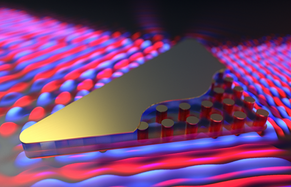
The OIST team’s experimental setup consists of two lasers that produce light at different wavelengths, an optical nanofiber used to guide light, and rubidium atoms trapped around it. The peculiarity of optical nanofibers is their super-thin diameter. For this study the diameter was 350 nanometers, about 300 times thinner than the thickness of a sheet of paper. The diameter is even smaller than the wavelength of the light guided by the fiber. Some of the light, therefore, leaks outside the nanofiber and interacts with the rubidium atoms that are trapped around it. These atoms can function as a quantum node, a redistribution point of a network, the equivalent of today’s servers.

The off switch condition is obtained when only the laser producing 780 nm is on. In this case, at the point where light leaks outside of the optical nanofiber, the rubidium atoms absorb the maximum amount of light and almost no light can continue to pass along the fiber. In contrast, the switch is turned on when both 776 nm and 780 nm lights are present. In this situation, most of the light is transmitted through the optical nanofiber and the rubidium atoms absorb it only minimally.

Since the optical nanofiber is directly connected to a standard optical fiber, the light can, in principle, be transferred to another quantum system or node some distance away, in the same way you can send a message from your computer to that of your friend’s in another location. 

“Using optical nanofibers would allow us to fully integrate our system with existing fiber-based communication networks. While the current work is far from being a practical solution to quantum information, it brings the notion of using atoms and light to develop real devices based on quantum mechanics ever closer to fulfilment”, explains Professor Síle Nic Chormaic.

While the experiment at OIST currently only generates zeros/off and ones/on consecutively, further exploitation of the quantum behavior of atoms should allow the research team to send light as a combination of “on” and “off” at the same time. In this way, in the future, quantum networks will be able to process more data simultaneously, increase efficiency of information transfer and also provide better cyber security.

“It has been very exciting to work with optical nanofibers which can guide light extremely efficiently even if their diameter is much smaller than the wavelength of light itself. These systems are sure to give us significant progress in quantum networks in the years to come,” enthuses Ravi Kumar, one of the authors of this study and a PhD student at University College Cork in Ireland, doing his research work at OIST.

Friday, December 4, 2015

Scientists Dramatically Increase Light from Atomic-Sized Materials


A recent article in the journalScience details how researchers from the Erik Jonsson School of Engineering and Computer Sciencedevised a simple process that dramatically increases light generation from certain atomic-sized materials.

The findings could have a broad impact in the advancement of LED displays, high efficiency solar cells, photo detectors, and nano-electronic circuits and devices.

“The prospect of using atomically thin materials for electronic applications that can detect and control light emission, what is known as optoelectronics, has captured the imagination of scientists and researchers across the world,” said co-author Dr. Robert Wallace, professor of materials science and engineering, and Erik Jonsson Distinguished Chair. 

Alongside a team of international collaborators, the UT Dallas scientists focused their research on a class of materials called transition metal dichalcogenides (TMDs), which can form an atomically thin layer that behaves like a semiconductor switch. For optoelectronic applications, a big hurdle to further development of TMD-based devices has been the low efficiency of their light generation.  
The article in Science shows how the efficiency of light generation in a particular TMD, molybdenum disulfide, can be improved by more than 100 times.

“Typically, this efficiency is captured in a benchmark measurement called ‘quantum yield,’” Wallace said. “Quantum yields are typically less than 1 percent for these atomically thin layered materials, making useful optoelectronic devices impractical. The low yield is thought to originate from imperfections in the TMD layer that results in mediocre electronic quality.”

Despite the typical low yield percentages, the researchers found that a relatively simple wet chemical treatment improves the performance of molybdenum disulfide, resulting in quantum yield of around 95 percent.

Collaborators at the University of California, Berkeley, led by Dr. Ali Javey, originally observed the extremely enhanced quantum yields upon exposure to the chemical treatment, which involves the use of an air-stable, solution-based organic superacid. 

“The improvement observed was intriguing and we were eager to better understand how the treatment improves the efficiency,” Wallace said.

As the chemical treatment is straightforward and easy to adopt, it is expected to significantly impact a wide range of TMD materials and device research and development.

Dr. Kyeongjae “K.J.” Cho, professor of materials science and engineering, said that as computer chips and other components become smaller, that the need for efficient nano-electronic circuits and devices becomes greater.

“In addition to improved optoelectronic devices, such as photodetectors and light-emitting diodes, this discovery will impact performance in other components like transistors,” Cho said.

Other UT Dallas co-authors included graduate students Angelica Azcatl and Dr. Santosh KC, research scientist Dr. Rafik Addou and postdoctoral research associate Dr. Jiyoung Noh. The UT Dallas team was called upon to provide the detailed materials characterization and modeling of the superacid treatment.

“The modeling and characterization study at UT Dallas provides key insights on the underlying mechanisms leading to the improvement in the efficiency,” Cho said.

Work at UT Dallas was supported through the Center for Low Energy Systems Technology, one of six centers supported by the STARnet phase of the Focus Center Research Program — a Semiconductor Research Corporation program sponsored by Microelectronics Advanced Research Corporation and the Defense Advanced Research Projects Agency.

Earlier in this semester, Wallace also was involved in a study that showed TMDs exhibited a quantum mechanical behavior called negative differential resistance, or NDR, at room temperature when grown as a layered structure. NDR is a phenomenon in which electrons, due to their wave nature, tunnel through thin materials with varying resistance.

Monday, November 30, 2015

Tapping Particles of Light


At the Weizmann Institute of Science, researchers have managed to “pluck” a single photon – one particle of light – out of a pulse of light. The findings of this research,which appeared this week in Nature Photonics, bear both fundamental and practical significance: Light is the workhorse of today’s communication systems, and single photons are likely to be the backbone of future quantum communication systems. In addition, say the scientists, the apparatus they have devised will spur further research into the fundamental particle nature of light.  

“Once we move over to quantum communication, information will have to be encoded in single photons,” says Dr. Barak Dayan, head of the Weizmann Institute Quantum Optics group. “Each photon will then represent a single ‘qubit’ – a quantum bit that can exist in more than one state at the same time (for example, an equal combination of both 1 and 0).”

Dayan and his research team, led by Dr. Serge Rosenblum and Orel Bechler, set out to demonstrate a scheme for pulling just one photon out of a stream, on demand. Their mechanism relies on a physical effect that they call single-photon Raman interaction, or SPRINT, which is based on a single atom, or atom-like system. “The advantage of SPRINT,” says Dayan, “is that it is completely passive - it does not require any control fields, just the interaction between the atom and the optical pulse.” In previous research, he and his team had employed SPRINT as a switch for single photons that sent them down different pathways, effectively turning the apparatus into a photonic router. In this work, the atom becomes a tap rather than a switch, snatching one photon from the flow and then turning itself off. “It is not trivial,” says Dayan, “to have a mechanism that continues to function even in high fluxes of photons and to remove just one photon.” 

The experimental setup of Weizmann’s quantum optics group relies on state-of-the-art technologies: laser cooling and trapping of atoms (in this case rubidium), the fabrication of chip-based, ultrahigh-quality glass microspheres, and optical nanofibers. 

“The ability to divert a single photon from a flow could be harnessed for various tasks,” says Dayan, “from creating nonclassical states of light that are useful for basic scientific research, through eavesdropping on imperfect quantum-cryptography systems that rely on single photons, to increasing the security of your own quantum-communication systems. 

The existence of photons was first suggested by Einstein in 1905, yet many of their properties are just now coming to light. Dayan believes their new method will expand our capabilities to study and control them as individual particles.

Monday, October 19, 2015

To infinity and beyond: Light goes infinitely fast with new on-chip material


Electrons are so 20th century. In the 21st century, photonic devices, which use light to transport large amounts of information quickly, will enhance or even replace the electronic devices that are ubiquitous in our lives today. But there’s a step needed before optical connections can be integrated into telecommunications systems and computers: researchers need to make it easier to manipulate light at the nanoscale.  

Researchers at the Harvard John A. Paulson School of Engineering and Applied Sciences (SEAS) have done just that, designing the first on-chip metamaterial with a refractive index of zero, meaning that the phase of light can travel infinitely fast. 

This new metamaterial was developed in the lab of Eric Mazur, the Balkanski Professor of Physics and Applied Physics and Area Dean for Applied Physics at SEAS, and is described in the journal Nature Photonics.

“Light doesn’t typically like to be squeezed or manipulated but this metamaterial permits you to manipulate light from one chip to another, to squeeze, bend, twist and reduce diameter of a beam from the macroscale to the nanoscale,” said Mazur. “It’s a remarkable new way to manipulate light.”

Although this infinitely high velocity sounds like it breaks the rule of relativity, it doesn’t. Nothing in the universe travels faster than light carrying information — Einstein is still right about that. But light has another speed, measured by how fast the crests of a wavelength move, known as phase velocity. This speed of light increases or decreases depending on the material it’s moving through.

When light passes through water, for example, its phase velocity is reduced as its wavelengths get squished together. Once it exits the water, its phase velocity increases again as its wavelength elongates. How much the crests of a light wave slow down in a material is expressed as a ratio called the refraction index — the higher the index, the more the material interferes with the propagation of the wave crests of light. Water, for example, has a refraction index of about 1.3.

When the refraction index is reduced to zero, really weird and interesting things start to happen.
In a zero-index material, there is no phase advance, meaning light no longer behaves as a moving wave, traveling through space in a series of crests and troughs. Instead, the zero-index material creates a constant phase — all crests or all troughs — stretching out in infinitely long wavelengths.  The crests and troughs oscillate only as a variable of time, not space.

This uniform phase allows the light to be stretched or squished, twisted or turned, without losing energy. A zero-index material that fits on a chip could have exciting applications, especially in the world of quantum computing.  

“Integrated photonic circuits are hampered by weak and inefficient optical energy confinement in standard silicon waveguides,” said Yang Li, a postdoctoral fellow in the Mazur Group and first author on the paper. “This zero-index metamaterial offers a solution for the confinement of electromagnetic energy in different waveguide configurations because its high internal phase velocity produces full transmission, regardless of how the material is configured.” 

The metamaterial consists of silicon pillar arrays embedded in a polymer matrix and clad in gold film. It can couple to silicon waveguides to interface with standard integrated photonic components and chips.

“In quantum optics, the lack of phase advance would allow quantum emitters in a zero-index cavity or waveguide to emit photons which are always in phase with one another,” said Philip Munoz, a graduate student in the Mazur lab and co-author on the paper.  “It could also improve entanglement between quantum bits, as incoming waves of light are effectively spread out and infinitely long, enabling even distant particles to be entangled.”

“This on-chip metamaterial opens the door to exploring the physics of zero index and its applications in integrated optics,” said Mazur. 

Tuesday, October 13, 2015

Painting quantum electronics with beams of light


A team of scientists from the University of Chicago and Penn State University has accidentally discovered a new way of using light to draw and erase quantum-mechanical circuits in a unique class of materials called topological insulators.

In contrast to using advanced nanofabrication facilities based on chemical processing of materials, this flexible technique allows for rewritable “optical fabrication” of devices. This finding is likely to spawn new developments in emerging technologies such as low-power electronics based on the spin of electrons or ultrafast quantum computers. The research was published Oct. 9 in the American Association for the Advancement of Science’s new online journal Science Advances.

“This observation came as a complete surprise,” said David D. Awschalom, the Liew Family Professor and deputy director in the Institute of Molecular Engineering at UChicago, who was one of two lead researchers on the project. “It’s one of those rare moments in experimental science where a seemingly random event—turning on the room lights—generated unexpected effects with potentially important impacts in science and technology.” 

The electrons in topological insulators have unique quantum properties that many scientists believe will be useful for developing spin-based electronics and quantum computers. However, making even the simplest experimental circuits with these materials has proved difficult because traditional semiconductor engineering techniques tend to destroy their fragile quantum properties. Even a brief exposure to air can reduce their quality.

In Science Advances, the researchers report the discovery of an optical effect that allows them to “tune” the energy of electrons in these materials using light, and without ever having to touch the material itself. They have used it to draw and erase p-n junctions—one of the central components of a transistor—in a topological insulator for the first time.
Like many advances in science, the path to this discovery had an unexpected twist.

“To be honest, we were trying to study something completely different,” said Andrew Yeats, a graduate student in Awschalom’s laboratory and the paper’s lead author. “There was a slow drift in our measurements that we traced to a particular type of fluorescent lights in our lab. At first we were glad to be rid of it, and then it struck us—our room lights were doing something that people work very hard to do in these materials.”

The researchers went back to Bulley & Andrews Construction, the contractor that renovated the lab space, for more information about the lights. “I’ve never had a client so obsessed with the overhead lighting,” said Frank Floss, superintendent for Bulley & Andrews. “I could have never imagined how important it would turn out to be.”  

The researchers found that the surface of strontium titanate, the substrate material on which they had grown their samples, becomes electrically polarized when exposed to ultraviolet light, and their room lights happened to emit at just the right wavelength. The electric field from the polarized strontium titanate was leaking into the topological insulator layer, changing its electronic properties.

Awschalom and his colleagues found that by intentionally focusing beams of light on their samples, they could draw electronic structures that persisted long after the light was removed.
“It’s like having a sort of quantum Etch A Sketch in our lab,” he said. They also found that bright red light counteracted the effect of the ultraviolet light, allowing them to both write and erase.

“Instead of spending weeks in the cleanroom and potentially contaminating our materials,” said Awschalom, “now we can sketch and measure devices for our experiments in real time. When we’re done, we just erase it and make something else. We can do this in less than a second.”

To test whether the new technique might interfere with the unique properties of topological insulators, the team measured their samples in high magnetic fields. They found promising signatures of an effect called weak anti-localization, which arises from quantum interference between the different simultaneous paths that electrons can take through a material when they behave as waves.

“One exciting aspect of this work is that it’s noninvasive,” said Prof. Nitin Samarth, the George A. and Margaret M. Downsbrough Department Head of Physics at Penn State, and a lead researcher on the project. “Since the electrical polarization occurs in an adjacent material, and the effect persists in the dark, the topological insulator remains relatively undisturbed. With these fragile quantum materials, sometimes you have to use a light touch.”

To better understand the physics behind the effect, the researchers conducted a number of control measurements. They showed that the optical effect is not unique to topological insulators, but that it can act on other materials grown on strontium titanate as well.

“In a way, the most exciting aspect of this work is that it should be applicable to a wide range of nanoscale materials such as complex oxides, graphene and transition metal dichalcogenides,” said Awschalom. “It’s not just that it’s faster and easier. This effect could allow electrical tuning of materials in a wide range of optical, magnetic and spectroscopic experiments where electrical contacts are extremely difficult or simply impossible.”


Tuesday, September 15, 2015

Tracking slow nanolight in natural hyperbolic metamaterial slabs

Tracking slow nanolight in natural hyperbolic metamaterial slabs
Researchers at CIC nanoGUNE (Basque Country) in collaboration with colleagues at ICFO - The Institute of Photonic Sciences (Catalunya) have imaged how light moves inside an exotic class of matter known as hyperbolic materials. They observed, for the first time, ultraslow pulse propagation and backward propagating waves in deep subwavelength-scale thick slabs of boron nitride - a natural hyperbolic material for infrared light. This work has been funded by the EC Graphene Flagship and was recently reported in Nature Photonics.
Hyperbolic materials are very special because they behave like a metal in one direction, but like an insulator in the other. Until now, these materials have been used to fabricate complex nanostructures that permit subwavelength-scale imaging, as well as the focusing and controlling of light at the nanoscale. However, in order to fully exploit their potential, it is necessary to study and understand how light behaves inside them.
The work lays the foundations for studying the precise manner in which light travels through complex optical systems at the subwavelength scale in extremely high levels of detail. Such a capability will be vital for verifying that future nanophotonic devices, perhaps with biosensing or optical computing applications, are functioning as expected.
“The difficulty in performing the reported experiments is the extremely short wavelength of light when it is inside a hyperbolic material” explains Ikerbasque Professor Rainer Hillenbrand, leader of the nanooptics group at nanoGUNE. When light moves inside the material - in our case mid-infrared light in a 135 nm boron nitride slab - it travels in the form of what we call a polariton, where the light is actually coupled to the vibrations of the matter itself".