Showing posts with label computer science. Show all posts

Wednesday, December 9, 2015

Using Atoms to Turn Optical Nanofiber Guided Light On and Off


Researchers in the Light-Matter Interactions Unit led by Professor Síle Nic Chormaic at the Okinawa Institute of Science and Technology Graduate University (OIST) have developed an on-off switch with ultrathin optical fibers, which could be used for data transfer in the future. This research was published in the New Journal of Physics.

0101000001101000011110010111001101101001011000110111001100100000011010010111001100100000011001100111010101101110 means “Physics is fun” in binary code. Computers translate every letter, number, sign, space, image and sound to a set of 8 ones and zeros. For example, 01010000 corresponds to the letter P. While you type, your computer transfers your words to another distant computer by sending a series of ones and zeros encoded in light through standard optical fibers. Switching the light beam on and off very quickly generates the ones and zeros. These bits of information are converted to electronic signals at a node, usually a router or server, and finally appear as text on the screen of your recipient. While this is the classical way of transferring information online, OIST researchers are exploring more efficient ways of transferring data, using the quantum properties of light and matter. They have managed to create an on/off switch based on the quantum characteristics of rubidium atoms in the presence of light of different wavelengths. This proof-of-concept system could be used as a building block in a quantum network, the future of our internet.

The OIST team’s experimental setup consists of two lasers that produce light at different wavelengths, an optical nanofiber used to guide light, and rubidium atoms trapped around it. The peculiarity of optical nanofibers is their super-thin diameter. For this study the diameter was 350 nanometers, about 300 times thinner than the thickness of a sheet of paper. The diameter is even smaller than the wavelength of the light guided by the fiber. Some of the light, therefore, leaks outside the nanofiber and interacts with the rubidium atoms that are trapped around it. These atoms can function as a quantum node, a redistribution point of a network, the equivalent of today’s servers.

The off switch condition is obtained when only the laser producing 780 nm is on. In this case, at the point where light leaks outside of the optical nanofiber, the rubidium atoms absorb the maximum amount of light and almost no light can continue to pass along the fiber. In contrast, the switch is turned on when both 776 nm and 780 nm lights are present. In this situation, most of the light is transmitted through the optical nanofiber and the rubidium atoms absorb it only minimally.

Since the optical nanofiber is directly connected to a standard optical fiber, the light can, in principle, be transferred to another quantum system or node some distance away, in the same way you can send a message from your computer to that of your friend’s in another location. 

“Using optical nanofibers would allow us to fully integrate our system with existing fiber-based communication networks. While the current work is far from being a practical solution to quantum information, it brings the notion of using atoms and light to develop real devices based on quantum mechanics ever closer to fulfilment”, explains Professor Síle Nic Chormaic.

While the experiment at OIST currently only generates zeros/off and ones/on consecutively, further exploitation of the quantum behavior of atoms should allow the research team to send light as a combination of “on” and “off” at the same time. In this way, in the future, quantum networks will be able to process more data simultaneously, increase efficiency of information transfer and also provide better cyber security.

“It has been very exciting to work with optical nanofibers which can guide light extremely efficiently even if their diameter is much smaller than the wavelength of light itself. These systems are sure to give us significant progress in quantum networks in the years to come,” enthuses Ravi Kumar, one of the authors of this study and a PhD student at University College Cork in Ireland, doing his research work at OIST.

Wednesday, December 2, 2015

Quantum computer made of standard semiconductor materials

Magnetic field helps qubit electrons store information longer


Physicists at the Technical University of Munich, the Los Alamos National Laboratory and Stanford University (USA) have tracked down semiconductor nanostructure mechanisms that can result in the loss of stored information – and halted the amnesia using an external magnetic field. The new nanostructures comprise common semiconductor materials compatible with standard manufacturing processes.

Quantum bits, qubits for short, are the basic logical elements of quantum information processing (QIP) that may represent the future of computer technology. Since they process problems in a quantum-mechanical manner, such quantum computers might one day solve complex problems much more quickly than currently possible, so the hope of researchers.

In principle, there are various possibilities of implementing qubits: photons are an option equally as viable as confined ions or atoms whose states can be altered in a targeted manner using lasers. The key questions regarding their potential use as memory units are how long information can be stored in the system and which mechanisms might lead to a loss of information.

A team of physicists headed by Alexander Bechtold and Professor Jonathan Finley at the Walter Schottky Institute of the Technical University of Munich and the Excellence Cluster Nanosystems Initiative Munich (NIM) have now presented a system comprising a single electron trapped in a semiconductor nanostructure. Here, the electron’s spin serves as the information carrier.

The researchers were able to precisely demonstrate the existence of different data loss mechanisms and also showed that stored information can nonetheless be retained using an external magnetic field.

Electrons trapped in a quantum dot

The TUM physicists evaporated indium gallium arsenide onto a gallium arsenide substrate to form their nanostructure. As a result of the different lattice spacing of the two semiconductor materials strain is produced at the interface between the crystal grids. The system thus forms nanometer-scale “hills” – so-called quantum dots.

When the quantum dots are cooled down to liquid helium temperatures and optically excited, a singe electron can be trapped in each of the quantum dots. The spin states of the electrons can then be used as information stores. Laser pulses can read and alter the states optically from outside. This makes the system ideal as a building block for future quantum computers.

Spin up or spin down correspond to the standard logical information units 0 and 1. But, on top of this come additional intermediate states of quantum mechanical up and down superpositions.

Hitherto unknown memory loss mechanisms

However, there is one problem: “We found out that the strain in the semiconductor material leads to a new and until recently unknown mechanism that results in the loss of quantum information,” says Alexander Bechtold. The strain creates tiny electric fields in the semiconductor that influence the nuclear spin orientation of the atomic nuclei.

“It’s a kind of piezoelectric effect,” says Bechthold. “It results in uncontrolled fluctuations in the nuclear spins.” These can, in turn, modify the spin of the electrons, i.e. the stored information. The information is lost within a few hundred nanoseconds.

In addition, Alexander Bechthold’s team was able to provide concrete evidence for further information loss mechanisms, for example that electron spins are generally influenced by the spins of the surrounding 100,000 atomic nuclei.

Preventing quantum mechanical amnesia

“However, both loss channels can be switched off when a magnetic field of around 1.5 tesla is applied,” says Bechtold. “This corresponds to the magnetic field strength of a strong permanent magnet. It stabilizes the nuclear spins and the encoded information remains intact.”

“Overall, the system is extremely promising,” according to Jonathan Finley, head of the research group. “The semiconductor quantum dots have the advantage that they harmonize perfectly with existing computer technology since they are made of similar semiconductor material.” They could even be equipped with electrical contacts, allowing them to be controlled not only optically using a laser, but also using voltage pulses.

The research was funded by the European Union (S3 Nano and BaCaTeC), the US Department of Energy, the US Army Research Office (ARO), the German Research Foundation DFG (excellence cluster Nanosystems Munich (NIM) and SFB 631), the Alexander von Humboldt Foundation as well as the TUM Institute for Advanced Study (Focus Group Nanophotonics and Quantum Optics).

Publication:

Three-stage decoherence dynamics of an electron spin qubit in an optically active quantum dot; Alexander Bechtold, Dominik Rauch, Fuxiang Li, Tobias Simmet, Per-Lennart Ardelt, Armin Regler, Kai Müller, Nikolai A. Sinitsyn and Jonathan J. Finley; Nature Physics, 11, 1005-1008 (2015) – DOI: 10.1038/nphys3470

Monday, October 19, 2015

To infinity and beyond: Light goes infinitely fast with new on-chip material


Electrons are so 20th century. In the 21st century, photonic devices, which use light to transport large amounts of information quickly, will enhance or even replace the electronic devices that are ubiquitous in our lives today. But there’s a step needed before optical connections can be integrated into telecommunications systems and computers: researchers need to make it easier to manipulate light at the nanoscale.  

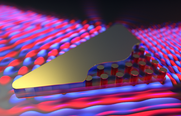
Researchers at the Harvard John A. Paulson School of Engineering and Applied Sciences (SEAS) have done just that, designing the first on-chip metamaterial with a refractive index of zero, meaning that the phase of light can travel infinitely fast. 

This new metamaterial was developed in the lab of Eric Mazur, the Balkanski Professor of Physics and Applied Physics and Area Dean for Applied Physics at SEAS, and is described in the journal Nature Photonics.

“Light doesn’t typically like to be squeezed or manipulated but this metamaterial permits you to manipulate light from one chip to another, to squeeze, bend, twist and reduce diameter of a beam from the macroscale to the nanoscale,” said Mazur. “It’s a remarkable new way to manipulate light.”

Although this infinitely high velocity sounds like it breaks the rule of relativity, it doesn’t. Nothing in the universe travels faster than light carrying information — Einstein is still right about that. But light has another speed, measured by how fast the crests of a wavelength move, known as phase velocity. This speed of light increases or decreases depending on the material it’s moving through.

When light passes through water, for example, its phase velocity is reduced as its wavelengths get squished together. Once it exits the water, its phase velocity increases again as its wavelength elongates. How much the crests of a light wave slow down in a material is expressed as a ratio called the refraction index — the higher the index, the more the material interferes with the propagation of the wave crests of light. Water, for example, has a refraction index of about 1.3.

When the refraction index is reduced to zero, really weird and interesting things start to happen.
In a zero-index material, there is no phase advance, meaning light no longer behaves as a moving wave, traveling through space in a series of crests and troughs. Instead, the zero-index material creates a constant phase — all crests or all troughs — stretching out in infinitely long wavelengths.  The crests and troughs oscillate only as a variable of time, not space.

This uniform phase allows the light to be stretched or squished, twisted or turned, without losing energy. A zero-index material that fits on a chip could have exciting applications, especially in the world of quantum computing.  

“Integrated photonic circuits are hampered by weak and inefficient optical energy confinement in standard silicon waveguides,” said Yang Li, a postdoctoral fellow in the Mazur Group and first author on the paper. “This zero-index metamaterial offers a solution for the confinement of electromagnetic energy in different waveguide configurations because its high internal phase velocity produces full transmission, regardless of how the material is configured.” 

The metamaterial consists of silicon pillar arrays embedded in a polymer matrix and clad in gold film. It can couple to silicon waveguides to interface with standard integrated photonic components and chips.

“In quantum optics, the lack of phase advance would allow quantum emitters in a zero-index cavity or waveguide to emit photons which are always in phase with one another,” said Philip Munoz, a graduate student in the Mazur lab and co-author on the paper.  “It could also improve entanglement between quantum bits, as incoming waves of light are effectively spread out and infinitely long, enabling even distant particles to be entangled.”

“This on-chip metamaterial opens the door to exploring the physics of zero index and its applications in integrated optics,” said Mazur. 

Monday, June 1, 2015

A new tool measures the distance between phonon collisions


Tabletop setup provides more nuanced picture of heat production in microelectronics.
Today’s computer chips pack billions of tiny transistors onto a plate of silicon within the width of a fingernail. Each transistor, just tens of nanometers wide, acts as a switch that, in concert with others, carries out a computer’s computations. As dense forests of transistors signal back and forth, they give off heat — which can fry the electronics, if a chip gets too hot.
Manufacturers commonly apply a classical diffusion theory to gauge a transistor’s temperature rise in a computer chip. But now an experiment by MIT engineers suggests that this common theory doesn’t hold up at extremely small length scales. The group’s results indicate that the diffusion theory underestimates the temperature rise of nanoscale heat sources, such as a computer chip’s transistors. Such a miscalculation could affect the reliability and performance of chips and other microelectronic devices.
“We verified that when the heat source is very small, you cannot use the diffusion theory to calculate temperature rise of a device. Temperature rise is higher than diffusion prediction, and in microelectronics, you don’t want that to happen,” says Professor Gang Chen, head of the Department of Mechanical Engineering at MIT. “So this might change the way people think about how to model thermal problems in microelectronics.”
The group, including graduate student Lingping Zeng and Institute Professor Mildred Dresselhaus of MIT, Yongjie Hu of the University of California at Los Angeles, and Austin Minnich of Caltech, has published its results this week in the journal Nature Nanotechnology.
Phonon mean free path distribution
Chen and his colleagues came to their conclusion after devising an experiment to measure heat carriers’ “mean free path” distribution in a material. In semiconductors and dielectrics, heat typically flows in the form of phonons — wavelike particles that carry heat through a material and experience various scatterings during their propagation. A phonon’s mean free path is the distance a phonon can carry heat before colliding with another particle; the longer a phonon’s mean free path, the better it is able to carry, or conduct, heat.
As the mean free path can vary from phonon to phonon in a given material — from several nanometers to microns — the material exhibits a mean free path distribution, or range. Chen, the Carl Richard Soderberg Professor in Power Engineering at MIT, reasoned that measuring this distribution would provide a more detailed picture of a material’s heat-carrying capability, enabling researchers to engineer materials, for example, using nanostructures to limit the distance that phonons travel.
The group sought to establish a framework and tool to measure the mean free path distribution in a number of technologically interesting materials. There are two thermal transport regimes: diffusive regime and quasiballistic regime. The former returns the bulk thermal conductivity, which masks the important mean free path distribution. To study phonons’ mean free paths, the researchers realized they would need a small heat source compared with the phonon mean free path to access the quasiballistic regime, as larger heat sources would essentially mask individual phonons’ effects.
Creating nanoscale heat sources was a significant challenge: Lasers can only be focused to a spot the size of the light’s wavelength, about one micron — more than 10 times the length of the mean free path in some phonons. To concentrate the energy of laser light to an even finer area, the team patterned aluminum dots of various sizes, from tens of micrometers down to 30 nanometers, across the surface of silicon, silicon germanium alloy, gallium arsenide, gallium nitride, and sapphire. Each dot absorbs and concentrates a laser’s heat, which then flows through the underlying material as phonons.
In their experiments, Chen and his colleagues used microfabrication to vary the size of the aluminum dots, and measured the decay of a pulsed laser reflected from the material — an indirect measure of the heat propagation in the material. They found that as the size of the heat source becomes smaller, the temperature rise deviates from the diffusion theory.
They interpret that as the metal dots, which are heat sources, become smaller, phonons leaving the dots tend to become “ballistic,” shooting across the underlying material without scattering. In these cases, such phonons do not contribute much to a material’s thermal conductivity. But for much larger heat sources acting on the same material, phonons tend to collide with other phonons and scatter more often. In these cases, the diffusion theory that is currently in use becomes valid.
A detailed transport picture
For each material, the researchers plotted a distribution of mean free paths, reconstructed from the heater-size-dependent thermal conductivity of a material. Overall, they observed the anticipated new picture of heat conduction: While the common, classical diffusion theory is applicable to large heat sources, it fails for small heat sources. By varying the size of heat sources, Chen and his colleagues can map out how far phonons travel between collisions, and how much they contribute to heat conduction.
Zeng says that the group’s experimental setup can be used to better understand, and potentially tune, a material’s thermal conductivity. For example, if an engineer desires a material with certain thermal properties, the mean free path distribution could serve as a blueprint to design specific “scattering centers” within the material — locations that prompt phonon collisions, in turn scattering heat propagation, leading to reduced heat carrying ability. Although such effects are not desirable in keeping a computer chip cool, they are suitable in thermoelectric devices, which convert heat to electricity. For such applications, materials that are electrically conducting but thermally insulating are desired.
“The important thing is, we have a spectroscopy tool to measure the mean free path distribution, and that distribution is important for many technological applications,” Zeng says.
This research was funded in part by in part by MIT’s Solid-State Solar Thermal Energy Conversion Center, which is funded by U.S. Department of Energy.
Source: http://newsoffice.mit.edu/2015/measuring-distance-between-phonon-collisions-0601