Showing posts with label nanoscale structures. Show all posts

Thursday, January 7, 2016

A Nanoscale Look at Why a New Alloy is Amazingly Tough


Just in time for the icy grip of winter: A team of researchers led by scientists from the U.S. Department of Energy Lawrence Berkeley National Laboratory (Berkeley Lab) has identified several mechanisms that make a new, cold-loving material one of the toughest metallic alloys ever.

The alloy is made of chromium, manganese, iron, cobalt and nickel, so scientists call it CrMnFeCoNi. It’s exceptionally tough and strong at room temperature, which translates into excellent ductility, tensile strength, and resistance to fracture. And unlike most materials, the alloy becomes tougher and stronger the colder it gets, making it an intriguing possibility for use in cryogenic applications such as storage tanks for liquefied natural gas.

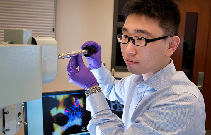
To learn its secrets, the Berkeley Lab-led team studied the alloy with transmission electron microscopy as it was subjected to strain. The images revealed several nanoscale mechanisms that activate in the alloy, one after another, which together resist the spread of damage. Among the mechanisms are bridges that form across cracks to inhibit their propagation. Such crack bridging is a common toughening mechanism in composites and ceramics but not often seen in unreinforced metals.

Their findings could guide future research aimed at designing metallic materials with unmatched damage tolerance. The research appears in the December 9, 2015, issue of the journal Nature Communications.

“We analyzed the alloy in earlier work and found spectacular properties: high toughness and strength, which are usually mutually exclusive in a material,” says Robert Ritchie, a scientist with Berkeley Lab’s Materials Sciences Division who led the research with Qian Yu of China’s Zhejiang University and several other scientists.

“So in this research, we used TEM to study the alloy at the nanoscale to see what’s going on,” says Ritchie.

In materials science, toughness is a material’s resistance to fracture, while strength is a material’s resistance to deformation. It’s very rare for a material to be both highly tough and strong, but CrMnFeCoNi isn’t a run-of-the-mill alloy. It’s a star member of a new class of alloys developed about a decade ago that contains five or more elements in roughly equal amounts. In contrast, most conventional alloys have one dominant element. These new multi-component alloys are called high-entropy alloys because they consist primarily of a simple solid solution phase, and therefore have a high entropy of mixing.

They’re a hot topic in materials research, and have only recently been available in a quality suitable for study. In 2014, Ritchie and colleagues found that at very cold temperatures, when CrMnFeCoNi deforms, a phenomenon called “twinning” occurs, in which adjacent crystalline regions form mirror arrangements of one another. Twinning likely plays a part in the alloy’s incredible toughness and strength. But twinning isn’t extensively found in the alloy at room temperature (except in the crack bridges), yet the alloy’s toughness and strength is still almost off the charts.

“If we don’t see twinning at room temperature, then what other mechanisms give the alloy these amazing properties?” asks Ritchie.

To find out, the scientists subjected the alloy to several straining experiments at room temperature, and used transmission electron microscopy to observe what happens.

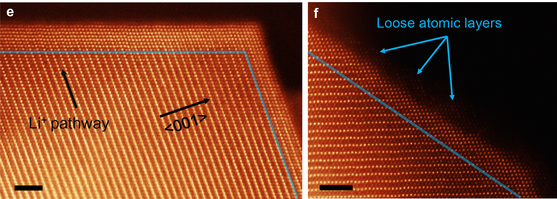
Their time-lapse images revealed two phenomena related to shear stress: slow-moving perfect dislocations that give the material strength, and fast-moving partial dislocations that enhance ductility. They also saw a phenomenon involving partial dislocations called “three-dimensional stacking fault defects,” in which the 3-D arrangement of atoms in a region changes. These faults are big barriers to dislocation, like placing a stack of bricks in front of a growing fissure, and serve to harden the alloy.

The images also captured the nanoscale version of chewing a mouthful of toffee and having your teeth stick together: In some cases, tiny bridges deformed by twinning are generated across a crack, which help prevent the crack from growing wider.

“These bridges are common in reinforced ceramics and composites,” says Ritchie. “Our research found that all of these nanoscale mechanisms work together to give the alloy its toughness and strength.”

Thursday, May 29, 2014

Scientists Pinpoint the Creeping Nanocrystals Behind Lithium-Ion Battery Degradation


Two breakthrough studies track the nanoscale structural changes that degrade battery performance during cycles of charge and discharge
Huolin Xin
Materials scientist Huolin Xin in Brookhaven Lab's Center for Functional Nanomaterials.
Batteries do not age gracefully. The lithium ions that power portable electronics cause lingering structural damage with each cycle of charge and discharge, making devices from smartphones to tablets tick toward zero faster and faster over time. To stop or slow this steady degradation, scientists must track and tweak the imperfect chemistry of lithium-ion batteries with nanoscale precision.
“We discovered surprising and never-before-seen evolution and degradation patterns in two key battery materials,” said Huolin Xin, a materials scientist at Brookhaven Lab’s Center for Functional Nanomaterials (CFN) and coauthor on both studies. “Contrary to large-scale observation, the lithium-ion reactions actually erode the materials non-uniformly, seizing upon intrinsic vulnerabilities in atomic structure in the same way that rust creeps unevenly across stainless steel.”In two recent Nature Communicationspapers, scientists from several U.S. Department of Energy national laboratories—Lawrence Berkeley, Brookhaven, SLAC, and the National Renewable Energy Laboratory—collaborated to map these crucial billionths-of-a-meter dynamics and lay the foundation for better batteries.
Scientists used electron tomography techniques to create this 3D animation of the nickel-oxide nanosheet transformations during the lithium-ion battery charging process.
Xin used world-leading electron microscopy techniques in both studies to directly visualize the nanoscale chemical transformations of battery components during each step of the charge-discharge process. In an elegant and ingenious setup, the collaborations separately explored a nickel-oxide anode and a lithium-nickel-manganese-cobalt-oxide cathode—both notable for high capacity and cyclability—by placing samples inside common coin-cell batteries running under different voltages.
“Armed with a precise map of the materials’ erosion, we can plan new ways to break the patterns and improve performance,” Xin said.
In these experiments, lithium ions traveled through an electrolyte solution, moving into an anode when charging and a cathode when discharging. The processes were regulated by electrons in the electrical circuit, but the ions’ journeys—and the battery structures—subtly changed each time.

Chinks in Nano-Armor

For the nickel-oxide anode, researchers submerged the batteries in a liquid organic electrolyte and closely controlled the charging rates. They stopped at predetermined intervals to extract and analyze the anode. Xin and his collaborators rotated 20-nanometer-thick sheets of the post-reaction material inside a carefully calibrated transmission electron microscope (TEM) grid at CFN to catch the contours from every angle—a process called electron tomography.
experimental coin cell setup
In the experimental coin cell setup, a carbon supported transmission electron microscopy (TEM) grid loaded with a small amount of the nickel-oxide material was pressed against the bulk anode and submerged in the same electrolyte environment.
To see the way the lithium-ions reacted with the nickel oxide, the scientists used a suite of custom-written software to digitally reconstruct the three-dimensional nanostructures with single-nanometer resolution. Surprisingly, the reactions sprang up at isolated spatial points rather than sweeping evenly across the surface.
“Consider the way snowflakes only form around tiny particles or bits of dirt in the air,” Xin said. “Without an irregularity to glom onto, the crystals cannot take shape. Our nickel oxide anode only transforms into metallic nickel through nanoscale inhomogeneities or defects in the surface structure, a bit like chinks in the anode’s armor.”
The electron microscopy provided a crucial piece of the larger puzzle assembled in concert with Berkeley Lab materials scientists and soft x-ray spectroscopy experiments conducted at SLAC’s Stanford Synchrotron Radiation Lightsource (SSRL). The combined data covered the reactions on the nano-, meso-, and microscales.

Rock-Salt Buildups

In the other study, scientists sought the voltage sweet-spot for the high-performing lithium-nickel-manganese-cobalt-oxide (NMC) cathode: How much power can be stored, at what intensity, and across how many cycles?
The answers hinged on intrinsic material qualities and the structural degradation caused by cycles at 4.7 volts and 4.3 volts, as measured against a lithium metal standard.
As revealed through another series of coin-cell battery tests, 4.7 volts caused rapid decomposition of the electrolytes and poor cycling—the higher power comes at a price. A 4.3-volt battery, however, offered a much longer cycling lifetime at the cost of lower storage and more frequent recharges.
In both cases, the chemical evolution exhibited sprawling surface asymmetries, though not without profound patterns.
atomic column in the NMC cathode
Each orange dot in these scanning transmission electron microscopy (STEM) images represents one atomic column in the NMC cathode. The scientists found that the lithium ions tended to travel along the vertical channels between atomic layers. After one full charge/discharge cycle, the surface layers (the edge beyond the blue line) exhibited the atomic disordering that ultimately diminishes battery performance.
“As the lithium ions race through the reaction layers, they cause clumping crystallization—a kind of rock-salt matrix builds up over time and begins limiting performance,” Xin said. “We found that these structures tended to form along the lithium-ion reaction channels, which we directly visualized under the TEM. The effect was even more pronounced at higher voltages, explaining the more rapid deterioration.”
Identifying this crystal-laden reaction pathways hints at a way forward in battery design.
“It may be possible to use atomic deposition to coat the NMC cathodes with elements that resist crystallization, creating nanoscale boundaries within the micron-sized powders needed at the cutting-edge of industry,” Xin said. “In fact, Berkeley Lab battery experts Marca Doeff and Feng Lin are working on that now.”
Shirley Meng, a professor at UC San Diego’s Department of NanoEngineering, added, “This beautiful study combines several complementary tools that probe both the bulk and surface of the NMC layered oxide—one of the most promising cathode materials for high-voltage operation that enables higher energy density in lithium-ion batteries. The meaningful insights provided by this study will significantly impact the optimization strategies for this type of cathode material.”
The TEM measurements revealed the atomic structures while electron energy loss spectroscopy helped pinpoint the chemical evolution—both carried out at the CFN. Further crucial research was conducted at SLAC’s SSRL and Berkeley Lab’s National Center for Materials Synthesis, Electrochemistry, and Electron Microscopy, with computational support from the National Energy Research Supercomputer Center and the Extreme Science and Engineering Discovery Environment.  

Toward Real-Time, Real-World Analyses

“The chemical reactions involved in these batteries are startlingly complex, and we need even more advanced methods of interrogation,” Xin said. “My CFN colleagues are developing ways to watch the reactions in real-time rather than the stop-and-go approach we used in these studies.” 
These in operando microscopy techniques, led in part by Brookhaven Lab materials scientists Dong Su, Feng Wang, and Eric Stach, will image reactions as they unfold in liquid environments. Custom-designed electrochemical contacts and liquid flow holders will usher in unprecedented insights.
Research at Brookhaven Lab’s CFN and SLAC’s SSRL—both DOE user facilities—was supported by DOE’s Office of Science. The NMC work was also supported through the Batteries for Advanced Transportation Technologies (BATT) program funded by DOE’s Office of Energy Efficiency and Renewable Energy and led by Berkeley Lab.
DOE's Office of Science is the single largest supporter of basic research in the physical sciences in the United States, and is working to address some of the most pressing challenges of our time. For more information, please visit science.energy.gov.
http://www.bnl.gov/newsroom/news.php?a=24805

Monday, May 26, 2014

Fractal Nanotruss Work


Fancy Erector Set? Nope. The elaborate fractal structure shown at right is many, many times smaller than that and is certainly not child's play. It is the latest example of what Julia Greer, professor of materials science and mechanics, calls a fractal nanotruss—nano because the structures are made up of members that are as thin as five nanometers (five billionths of a meter); truss because they are carefully architected structures that might one day be used in structural engineering materials.


Greer's group has developed a three-step process for building such complex structures very precisely. They first use a direct laser writing method called two-photon lithography to "write" a three-dimensional pattern in a polymer, allowing a laser beam to crosslink and harden the polymer wherever it is focused. At the end of the patterning step, the parts of the polymer that were exposed to the laser remain intact while the rest is dissolved away, revealing a three-dimensional scaffold. Next, the scientists coat the polymer scaffold with a continuous, very thin layer of a material—it can be a ceramic, metal, metallic glass, semiconductor, "just about anything," Greer says. In this case, they used alumina, or aluminum oxide, which is a brittle ceramic, to coat the scaffold. In the final step they etch out the polymer from within the structure, leaving a hollow architecture.

Taking advantage of some of the size effects that many materials display at the nanoscale, these nanotrusses can have unusual, desirable qualities. For example, intrinsically brittle materials, like ceramics, including the alumina shown, can be made deformable so that they can be crushed and still rebound to their original state without global failure.

"Having full control over the architecture gives us the ability to tune material properties to what was previously unattainable with conventional monolithic materials or with foams," says Greer. "For example, we can decouple strength from density and make materials that are both strong (and tough) as well as extremely lightweight. These structures can contain nearly 99 percent air yet can also be as strong as steel. Designing them into fractals allows us to incorporate hierarchical design into material architecture, which promises to have further beneficial properties."

The members of Greer's group who helped develop the new fabrication process and created these nanotrusses are graduate students Lucas Meza and Lauren Montemayor and Nigel Clarke, an undergraduate intern from the University of Waterloo.
Written by Kimm Fesenmaier

Source: http://www.caltech.edu/content/miniature-truss-work#sthash.xl98f5Tu.dpuf

Thursday, October 24, 2013

The Reins of Casimir: Engineered Nanostructures Could Offer Way to Control Quantum Effect ... Once a Mystery Is Solved

You might think that a pair of parallel plates hanging motionless in a vacuum just a fraction of a micrometer away from each other would be like strangers passing in the night—so close but destined never to meet. Thanks to quantum mechanics, you would be wrong.
casimir attraction illustration
Researchers measured the Casimir attraction between a metallic grating and a gold coated sphere. They found that the attraction between the nanostructured surface and the sphere decreased much more rapidly than theory predicts when the two surfaces were moved away from each other.
Credit: D. Lopez/Argonne
Scientists working to engineer nanoscale machines know this only too well as they have to grapple with quantum forces and all the weirdness that comes with them. These quantum forces, most notably the Casimir effect, can play havoc if you need to keep closely spaced surfaces from coming together.
Controlling these effects may also be necessary for making small mechanical parts that never stick to each other, for building certain types of quantum computers, and for studying gravity at the microscale.
Now, a large collaborative research group involving scientists from a number of federal labs, including the National Institute of Standards and Technology (NIST), and major universities, has observed that these sticky effects can be increased or lessened by patterning one of the surfaces with nanoscale structures. The discovery, described in Nature Communications,* opens a new path for tuning these effects.
But as often happens with quantum phenomena, the work raises new questions even as it answers others.
One of the insights of quantum mechanics is that no space, not even outer space, is ever truly empty. It's full of energy in the form of quantum fluctuations, including fluctuating electromagnetic fields that seemingly come from nowhere and disappear just as fast.
Some of this energy, however, just isn't able to "fit" in the submicrometer space between a pair of electromechanical contacts. More energy on the outside than on the inside results in a kind of "pressure" called the Casimir force, which can be powerful enough to push the contacts together and stick.
Prevailing theory does a good job describing the Casimir force between featureless, flat surfaces and even between most smoothly curved surfaces. However, according to NIST researcher and co-author of the paper, Vladimir Aksyuk, existing theory fails to predict the interactions they observed in their experiment.
"In our experiment, we measured the Casimir attraction between a gold-coated sphere and flat gold surfaces patterned with rows of periodic, flat-topped ridges, each less than 100 nanometers across, separated by somewhat wider gaps with deep sheer-walled sides," says Aksyuk. "We wanted to see how a nanostructured metallic surface would affect the Casimir interaction, which had never been attempted with a metal surface before. Naturally, we expected that there would be reduced attraction between our grooved surface and the sphere, regardless of the distance between them, because the top of the grooved surface presents less total surface area and less material. However, we knew the Casimir force's dependence on the surface shape is not that simple."
Indeed, what they found was more complicated.
According to Aksyuk, when they increased the separation between the surface of the sphere and the grooved surface, the researchers found that the Casimir attraction decreased much more quickly than expected. When they moved the sphere farther away, the force fell by a factor of two below the theoretically predicted value. When they moved the sphere surface close to the ridge tops, the attraction per unit of ridge top surface area increased.
"Theory can account for the stronger attraction, but not for the too-rapid weakening of the force with increased separation," says Aksyuk. "So this is new territory, and the physics community is going to need to come up with a new model to describe it."
This work was performed in collaboration with scientists from Los Alamos National Laboratory; the University of Maryland, College Park; Argonne National Laboratory; and Indiana University – Purdue University, Indianapolis.