Showing posts with label green energy. Show all posts

Wednesday, March 9, 2016

Converting atmospheric carbon dioxide into batteries


An interdisciplinary team of scientists has worked out a way to make electric vehicles that are not only carbon neutral, but carbon negative, capable of actually reducing the amount of atmospheric carbon dioxide as they operate.

They have done so by demonstrating how the graphite electrodes used in the lithium-ion batteries that power electric automobiles can be replaced with carbon material recovered from the atmosphere.

The recipe for converting carbon dioxide gas into batteries is described in the paper titled "Carbon Nanotubes Produced from Ambient Carbon Dioxide for Environmentally Sustainable Lithium-Ion and Sodium-Ion Battery Anodes" published in the Mar. 2 issue of the journal ACS Central Science.

The unusual pairing of carbon dioxide conversion and advanced battery technology is the result of a collaboration between the laboratory of Assistant Professor of Mechanical Engineering Cary Pint at Vanderbilt University and Professor of Chemistry Stuart Licht at George Washington University.

The team adapted a solar-powered process that converts carbon dioxide into carbon so that it produces carbon nanotubes and demonstrated that the nanotubes can be incorporated into both lithium-ion batteries like those used in electric vehicles and electronic devices and low-cost sodium-ion batteries under development for large-scale applications, such as the electric grid.

"This approach not only produces better batteries but it also establishes a value for carbon dioxide recovered from the atmosphere that is associated with the end-user battery cost unlike most efforts to reuse CO2 that are aimed at low-valued fuels, like methanol, that cannot justify the cost required to produce them," said Pint.

The project builds upon a solar thermal electrochemical process (STEP) that can create carbon nanofibers from ambient carbon dioxide developed by the Licht group and described in the journal Nano Letters last August. STEP uses solar energy to provide both the electrical and thermal energy necessary to break down carbon dioxide into carbon and oxygen and to produce carbon nanotubes that are stable, flexible, conductive and stronger than steel.

"Our climate change solution is two fold: (1) to transform the greenhouse gas carbon dioxide into valuable products and (2) to provide greenhouse gas emission-free alternatives to today's industrial and transportation fossil fuel processes," said Licht. "In addition to better batteries other applications for the carbon nanotubes include carbon composites for strong, lightweight construction materials, sports equipment and car, truck and airplane bodies."


Joining forces with Pint, whose research interests are focused on using carbon nanomaterials for battery applications, the two laboratories worked together to show that the multi-walled carbon nanotubes produced by the process can serve as the positive electrode in both lithium-ion and sodium-ion batteries.

In lithium-ion batteries, the nanotubes replace the carbon anode used in commercial batteries. The team demonstrated that the carbon nanotubes gave a small boost to the performance, which was amplified when the battery was charged quickly. In sodium-ion batteries, the researchers found that small defects in the carbon, which can be tuned using STEP, can unlock stable storage performance over 3.5 times above that of sodium-ion batteries with graphite electrodes. Most importantly, both carbon-nanotube batteries were exposed to about 2.5 months of continuous charging and discharging and showed no sign of fatigue.

Depending on the specifications, making one of the two electrodes out of carbon nanotubes means that up to 40 percent of a battery could be made out of recycled CO2, Pint estimated. This does not include the outer protective packaging but he suggested that processes like STEP could eventually produce the packaging as well.

The researchers estimate that with a battery cost of $325 per kWh (the average cost of lithium-ion batteries reported by the Department of Energy in 2013), a kilogram of carbon dioxide has a value of about $18 as a battery material - six times more than when it is converted to methanol - a number that only increases when moving from large batteries used in electric vehicles to the smaller batteries used in electronics. And unlike methanol, combining batteries with solar cells provides renewable power with zero greenhouse emissions, which is needed to put an end to the current carbon cycle that threatens future global sustainability.

Licht also proposed that the STEP process could be coupled to a natural gas powered electrical generator. The generator would provide electricity, heat and a concentrated source of carbon dioxide that would boost the performance of the STEP process. At the same time, the oxygen released in the process could be piped back to the generator where it would boost the generator's combustion efficiency to compensate for the amount of electricity that the STEP process consumes. The end result could be a fossil fuel electrical power plant with zero net CO2 emissions.

"Imagine a world where every new electric vehicle or grid-scale battery installation would not only enable us to overcome the environmental sins of our past, but also provide a step toward a sustainable future for our children," said Pint. "Our efforts have shown a path to achieve such a future."

Friday, April 18, 2014

Flowing salt water over graphene generates electricity

Illustration of the experimental set-up
Institute of Nanoscience, Nanjing University of
Aeronautics and Astronautics

Graphene, the “wonder material” that has caught the interest of scientists globally, could be used to make microscopic hydroelectric systems capable of powering small electronic devices, a new study has found. 

Since its discovery in 2004, many experts have said graphene could change the world. It is the strongest material known to exist, though it is only one atom thick. It is remarkably pliable, almost transparent and an excellent conductor of electricity and heat 
The potential applications of graphene are many, though much of the excitement has focused on the possibility of making advanced, lightweight and superfast electronics. 
In 2013, the EU made available a €1 billion grant to researchers investigating the potential uses of the environmentally friendly “wonder material”, saying it could become as important as steel or plastics. Bill Gates’s philanthropic foundation has even paid for the development of a graphene-based condom.
Now, in the findings of an unprecedented study, researchers from the Nanjing University of Aeronautics and Astronautics in China have revealed that dragging small droplets of salt water along strips of graphene generates electricity. 
They found that the faster they dragged the droplet across the graphene strip, the higher the voltage they generated.
The scientists then scaled up the experiment, placing a droplet of copper chloride on a tilted graphene surface, generating a voltage of approximately 30 millivolts (mV) – a millivolt being one thousandth of a volt.
Though much more research is needed, the scientists say these nano-sized generators could power small devices. This is something far beyond current hydroelectric systems – which usually work on a much larger scale. 
A separate study, published in 2013, also suggested that buildings covered in graphene paint could harness sunlight to generate solar power.
Nature Nanotechnology, 2014. DOI: 10.1038/NNANO.2014.56 

Friday, March 28, 2014

Rainbow-catching waveguide could revolutionize energy technologies

The image shows a “multilayered waveguide taper array.”
The different wavelengths, or colors, are absorbed
by the waveguide tapers (thimble-shaped structures)
that together form an array.
By slowing and absorbing certain wavelengths of light, engineers open new possibilities in solar power, thermal energy recycling and stealth technology.

More efficient photovoltaic cells. Improved radar and stealth technology. A new way to recycle waste heat generated by machines into energy.

All may be possible due to breakthrough photonics research at the University at Buffalo.

The work, published March 28 in the journal Scientific Reports, explores the use of a nanoscale microchip component called a “multilayered waveguide taper array” that improves the chip’s ability to trap and absorb light.

Unlike current chips, the waveguide tapers (the thimble-shaped structures pictured above) slow and ultimately absorb each frequency of light at different places vertically to catch a “rainbow” of wavelengths, or broadband light.

The paper, “Broadband absorption engineering of hyperbolic metafilm patterns,” is here: http://bit.ly/1g72Is5.

“We previously predicted the multilayered waveguide tapers would more efficiently absorb light, and now we’ve proved it with these experiments,” says lead researcher Qiaoqiang Gan, PhD, UB assistant professor of electrical engineering. “This advancement could prove invaluable for thin-film solar technology, as well as recycling waste thermal energy that is a byproduct of industry and everyday electronic devices such as smartphones and laptops.”

Each multilayered waveguide taper is made of ultrathin layers of metal, semiconductors and/or insulators. The tapers absorb light in metal dielectric layer pairs, the so-called hyperbolic metamaterial. By adjusting the thickness of the layers and other geometric parameters, the tapers can be tuned to different frequencies including visible, near-infrared, mid-infrared, terahertz and microwaves.

The structure could lead to advancements in an array of fields.
For example, there is a relatively new field of advanced computing research called on-chip optical communication. In this field, there is a phenomenon known as crosstalk, in which an optical signal transmitted on one waveguide channel creates an undesired scattering or coupling effect on another waveguide channel. The multilayered waveguide taper structure array could potentially prevent this.

It could also improve thin-film photovoltaic cells, which are a promising because they are less expensive and more flexible that traditional solar cells. The drawback, however, is that they don’t absorb as much light as traditional cells. Because the multilayered waveguide taper structure array can efficiently absorb the visible spectrum, as well as the infrared spectrum, it could potentially boost the amount of energy that thin-film solar cells generate.
The multilayered waveguide taper array could help recycle waste heat generated by power plants and other industrial processes, as well as electronic devices such as televisions, smartphones and laptop computers.

“It could be useful as an ultra compact thermal-absorption, collection and liberation device in the mid-infrared spectrum,” says Dengxin Ji, a PhD student in Gan’s lab and first author of the paper.

It could even be used as a stealth, or cloaking, material for airplanes, ships and other vehicles to avoid radar, sonar, infrared and other forms of detection. “The multilayered waveguide tapers can be scaled up to tune the absorption band to a lower frequency domain and absorb microwaves efficiently,” says Haomin Song, another PhD student in Gan’s lab and the paper’s second author.

Additional authors of the paper include Haifeng Hu, Kai Liu, Xie Zeng and Nan Zhang, all PhD candidates in UB’s Department of Electrical Engineering.

The National Science Foundation sponsored the research.

Gan is a member of UB’s electrical engineering optics and photonics research group, which includes professors Alexander N. Cartwright (also UB vice president for research and economic development), Edward Furlani and Pao-Lo Liu; associate professor Natalia Litchinitser; and assistant professor Liang Feng.

The group carries out research in nanophotonics, biophotonics, hybrid inorganic/organic materials and devices, nonlinear and fiber optics, metamaterials, nanoplasmonics, optofluidics, microelectromechanical systems (MEMS), biomedical microelectromechanical systems (BioMEMs), biosensing and quantum information processing.

Source: http://www.buffalo.edu/news/releases/2014/03/049.html#sthash.9qx1DAsE.dpuf

Monday, March 3, 2014

How to harvest energy from Earth's infrared emissions

HARVARD PHYSICISTS PROPOSE A DEVICE TO CAPTURE ENERGY FROM EARTH’S INFRARED EMISSIONS TO OUTER SPACE

When the sun sets on a remote desert outpost and solar panels shut down, what energy source will provide power through the night? A battery, perhaps, or an old diesel generator? Perhaps something strange and new.

Physicists at the Harvard School of Engineering and Applied Sciences (SEAS) envision a device that would harvest energy from Earth’s infrared emissions into outer space.
Heated by the sun, our planet is warm compared to the frigid vacuum beyond. Thanks to recent technological advances, the researchers say, that heat imbalance could soon be transformed into direct-current (DC) power, taking advantage of a vast and untapped energy source.
Their analysis of the thermodynamics, practical concerns, and technological requirements will be published this week in the Proceedings of the National Academy of Sciences.
“It’s not at all obvious, at first, how you would generate DC power by emitting infrared light in free space toward the cold,” says principal investigator Federico Capasso, the Robert L. Wallace Professor of Applied Physics and Vinton Hayes Senior Research Fellow in Electrical Engineering at Harvard SEAS. “To generate power by emitting, not by absorbing light, that’s weird. It makes sense physically once you think about it, but it’s highly counterintuitive. We’re talking about the use of physics at the nanoscale for a completely new application.”
Harvard physicists Federico Capasso (left), Steven J. Byrnes (right), and Romain Blanchard propose a new way to harvest renewable energy. (Photo by Eliza Grinnell, SEAS Communications.)

Challenging convention
Capasso is a world-renowned expert in semiconductor physics, photonics, and solid-state electronics. He co-invented the infrared quantum-cascade laser in 1994, pioneered the field of bandgap engineering, and demonstrated an elusive quantum electrodynamical phenomenon called the repulsive Casimir force—work for which he has received the SPIE Gold Medal, the European Physical Society Prize for Quantum Electronics and Optics, and the Jan Czochralski Award for lifetime achievement. His research team seems to specialize in rigorously questioning dated assumptions about optics and electronics.
“The mid-IR has been, by and large, a neglected part of the spectrum,” says Capasso. “Even for spectroscopy, until the quantum cascade laser came about, the mid-IR was considered a very difficult area to work with. People simply had blinders on.”
Now, Capasso and his research team are proposing something akin to a photovoltaic solar panel, but instead of capturing incoming visible light, the device would generate electric power by releasing infrared light.
“Sunlight has energy, so photovoltaics make sense; you’re just collecting the energy. But it’s not really that simple, and capturing energy from emitting infrared light is even less intuitive,” says lead author Steven J. Byrnes (AB ’07), a postdoctoral fellow at SEAS. “It’s not obvious how much power you could generate this way, or whether it’s worthwhile to pursue, until you sit down and do the calculation.”
As it turns out, the power is modest but real.
As Byrnes points out, “The device could be coupled with a solar cell, for example, to get extra power at night, without extra installation cost.”
Two proposed devices—one macro, one nano
To show the range of possibilities, Capasso’s group suggests two different kinds of emissive energy harvesters: one that is analogous to a solar thermal power generator, and one that is analogous to a photovoltaic cell. Both would run in reverse.
The first type of device would consist of a “hot” plate at the temperature of the Earth and air, with a “cold” plate on top of it. The cold plate, facing upward, would be made of a highly emissive material that cools by very efficiently radiating heat to the sky. Based on measurements of infrared emissions in Lamont, Oklahoma (as a case study), the researchers calculate that the heat difference between the plates could generate a few watts per square meter, day and night. Keeping the “cold” plate cooler than the ambient temperature would be difficult, but this device illustrates the general principle: differences in temperature generate work.
“This approach is fairly intuitive because we are combining the familiar principles of heat engines and radiative cooling,” says Byrnes.  
The second proposed device relies on temperature differences between nanoscale electronic components—diodes and antennas—rather than a temperature that you could feel with your hand.
“If you have two components at the same temperature, obviously you can’t extract any work, but if you have two different temperatures you can,” says Capasso. “But it’s tricky; at the level of the electron behaviors, the explanation is much less intuitive.”
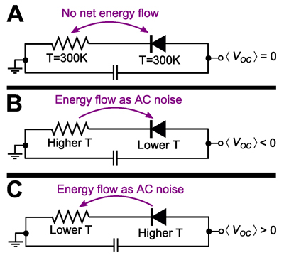
Three diode-resistor generator circuits with different temperature inputs. A circuit at thermal equilibrium (A) generates no current; (B) is a conventional rectifier circuit. The Harvard team proposes a twist—shown in (C). (Image courtesy of Federico Capasso and PNAS.)
“The key is in these beautiful circuit diagrams,” he adds (see image at right). “We found they had been considered before for another application—in 1968 by J.B. Gunn, the inventor of the Gunn diode used in police radars—and been completely buried in the literature and forgotten. But to try to explain them qualitatively took a lot of effort.”
Simply put, components in an electrical circuit can spontaneously push current in either direction; this is called electrical noise. Gunn’s diagrams show that if a valve-like electrical component called a diode is at a higher temperature than a resistor, it will push current in a single direction, producing a positive voltage. Capasso’s group suggests that the role of the resistor could be played by a microscopic antenna that very efficiently emits the Earth’s infrared radiation toward the sky, cooling the electrons in only that part of the circuit.
The result, says Byrnes, is that “you get an electric current directly from the radiation process, without the intermediate step of cooling a macroscopic object.”
According to the paper, a single flat device could be coated in many of these tiny circuits, pointed at the sky, and used to generate power.
Technological challenges—and promise
The optoelectronic approach, while novel, could be feasible in light of recent technological developments—advances in plasmonics, small-scale electronics, new materials like graphene, and nanofabrication. The Harvard team says a strength of their research is that it clarifies the remaining challenges.
“People have been working on infrared diodes for at least 50 years without much progress, but recent advances such as nanofabrication are essential to making them better, more scalable, and more reproducible,” says Byrnes.
We’re talking about the use of physics at the nanoscale for a completely new application.
However, even with the best modern infrared diodes, there is a problem. “The more power that’s flowing through a single circuit, the easier it is to get the components to do what you want. If you’re harvesting energy from infrared emissions, the voltage will be relatively low,” explains Byrnes. “That means it’s very difficult to create an infrared diode that will work well.”
Engineers and physicists, including Byrnes, are already considering new types of diodes that can handle lower voltages, such as tunnel diodes and ballistic diodes. Another approach would be to increase the impedance of the circuit components, thereby raising the voltage to a more practical level. The solution might require a little of both, Byrnes predicts.
Speed presents another challenge.  “Only a select class of diodes can switch on and off 30 trillion times a second, which is what we need for infrared signals,” says Byrnes. “We need to deal with the speed requirements at the same time we deal with the voltage and impedance requirements.”
“Now that we understand the constraints and specifications,” Byrnes adds, “we are in a good position to work on engineering a solution.”
Romain Blanchard, who completed his Ph.D. at Harvard SEAS, was also a coauthor of the paper in PNAS. This research was supported in part by King Abdullah University of Science and Technology.
Source: http://www.seas.harvard.edu/news/2014/03/infrared-new-renewable-energy-source

Monday, February 24, 2014

TU Delft achieves maximum light trapping in solar cells

Researchers at TU Delft have opened the way for the realization of the next generation of high-efficiency, cost-effective and ultra-thin crystalline silicon solar cells. They are the first in the world to come very close (99.8%) to the theoretical limit of absorption enhancement (light trapping) in a broad light spectrum range. Their article on light management in ultra-thin silicon is accepted for publication in the journal ACS Photonics.


PhD-student Andrea Ingenito of the Photovoltaic Materials and Devices (PVMD) group at TU Delft has experimentally demonstrated the theoretical limit of the enhancement of light absorption in a thin semiconductor material. Ingenito used wafers of crystalline silicon and experimentally proved the theoretical prediction of the maximal enhancement of light absorption in a semiconductor material. He is the first in the world to come very close (99.8%) to the theoretical limit of absorption enhancement in a broad light spectrum range. An experimental demonstration of this absorption enhancement limit in solar cells has been elusive for the last thirty years.


The PVMD group at TU Delft (Faculty of EEMCS) has world-leading expertise in the design, fabrication, and implementation of light trapping structures in the solar cells. The researchers in the group managed to develop an advanced metal-free light trapping scheme for crystalline silicon wafers. At the front side of the silicon wafers they applied a nano-texture known as black-silicon. At the rear side, they implemented a random pyramidal texture coated with a photonic Dielectric Back Reflector which was designed to exhibit maximal and omni-directional internal reflectance. For wafers thinner than 35 μm the researchers achieved more than 99% (with the photonic reflector) and up to 99.8% (with the silver back reflector) of the theoretical classical absorption limit in the broad light spectrum from 400 to 1200 nm.


Successful implementation of TU Delft’s light trapping scheme in crystalline silicon solar cells requires an adequate surface passivation of the front nano-texture. For this purpose, the researchers at the PVMD group have developed thermal silicon oxide and aluminium oxide passivation layers. TU Delft's trapping scheme together with excellent surface passivation opens the way for the realization of the next generation of high-efficiency, cost-effective and ultra-thin crystalline silicon solar cells.

Ingenito’s article in ACS Photonics was co-authored by supervisors prof. dr. Miro Zeman and dr. Olindo Isabella. The research was carried out in the AdLight project (Advanced light trapping for thin and highly efficient silicon solar cells) funded by Agentschap NL. Solland and ECN have been the partners in the project.

Source: http://www.tudelft.nl/en/current/latest-news/article/detail/tu-delft-realiseert-maximale-light-trapping-in-zonnecellen/

Wednesday, January 22, 2014

From a carpet of nanorods to a thin film solar cell absorber within a few seconds

The transformation from a layer of closely packed nanorods
(top left) to a polycrystalline semiconductor thin film (top right)
can be observed in by in-situ X-ray diffraction in real time.
The intensities of the diffraction signals are color coded in the
image at the bottom. A detailed analysis of the signals reveals
that the transformation of the nanorods into kesterite crystals
takes only 9 to 18 seconds.
Picture: R. Mainz/A. Singh
Research teams at the HZB and at the University of Limerick, Ireland, have discovered a novel solid state reaction which lets kesterite grains grow within a few seconds and at relatively low temperatures. For this reaction they exploit a transition from a metastable wurtzite compound in the form of nanorods to the more stable kesterite compound. 
At the EDDI Beamline at BESSY II, the scientists could observe this process in real-time when heating the sample: in a few seconds Kesterite grains formed. The size of the grains was found to depend on the heating rate. With fast heating they succeeded in producing a Kesterite thin film with near micrometer-sized crystal grains, which could be used in thin film solar cells. These findings have now been published in the journal “Nature Communications”.

Grain formation during growth of kesterite solar cells observed in real-time

As starting material for the formation of the kesterite film serves a “carpet of nanorods”: With the help of solution-based chemical processing, the chemists around Ajay Singh and Kevin Ryan at the University of Limerick have fabricated films of highly ordered wurtzite nanorods, which have exactly the same composition as kesterite Cu2ZnSnS4. With the help of real-time X-ray diffraction at the EDDI beamline of BESSY II, HZB physicists around Roland Mainz and Thomas Unold could now observe how a phase transition from the metastable wurtzite phase to the stable kesterite phase leads to a rapid formation of a thin film with large kesterite grains. “It is interesting to see that the complete formation of the kesterite film is so fast”, says Mainz. And the faster the samples are heated up, the larger the grains grow. Mainz explains that at low heating rate, the transition from wurtzite to kesterite starts at lower temperature at which many small grains form – instead of a few larger grains. Additionally, more defects are formed at lower temperatures. During fast heating, the transition takes place at higher temperature at which grains with less defects form.
Moreover, the comparison of the time-resolved evolution of the phase transition during slow and during fast heating shows that not only the grain growth is triggered by the phase transition, but also the phase transition is additionally accelerated by the grain growth. The HZB physicists have developed a model which can explain these findings. By means of numerical model calculations, they demonstrated the accordance of the model with the measured data.
Novel synthesis pathway for thin film semiconductors with controlled morphology
The work points towards a new pathway for the fabrication of thin microcrystalline semiconductor films without the need of expensive vacuum technology. Cu2ZnSnS4-based kesterite semiconductors have gained increasing attention in the past, since they are a promising alternative for the Cu(In,Ga)Se2chalcopyrite solar cells which already achieved efficiencies above 20%. Kesterite has similar physical properties as the chalcopyrite semiconductors, but consist only of elements which are abundantly present in the earth crust. The new procedure could also be interesting for the fabrication of micro- and nanostructured photoelectric devices as well as for semiconductor layers consisting of other materials, says Mainz. “But we continue to focus on kesterites, because this is a really exciting topic at the moment.”
Source: http://www.helmholtz-berlin.de/pubbin/news_seite?nid=13909;sprache=en;typoid=3228

Thursday, November 28, 2013

Nanoscale Coatings Improve Stability and Efficiency of Devices for Renewable Fuel Generation

A graphic representation of how atomic layer
deposition can aid renewable hydrogen fuel
generation. Two papers published in
Proceedings of the National Academy of
Sciences show how atomic layer deposition
can make water-splitting devices more stable and
more efficient.
Splitting water into its components, two parts hydrogen and one part oxygen, is an important first step in achieving carbon-neutral fuels to power our transportation infrastructure – including automobiles and planes.

Now, North Carolina State University researchers and colleagues from the University of North Carolina at Chapel Hill have shown that a specialized coating technique can make certain water-splitting devices more stable and more efficient. Their results are published online this week in two separate papers in the Proceedings of the National Academy of Sciences.

Atomic layer deposition, or “ALD,” coats three-dimensional structures with a precise, ultra-thin layer of material. “An ALD coating is sort of like the chocolate glaze on the outside of a Klondike bar – just much, much thinner,” explains Dr. Mark Losego, research assistant professor of chemical and biomolecular engineering at NC State and a co-author on the work. “In this case, the layers are less than one nanometer thick – or almost a million times thinner than a human hair.”

Although extremely thin, these coatings improve the attachment and performance of surface-bound molecular catalysts used for water-splitting reactions in hydrogen-fuel-producing devices.

In the first paper, “Solar water splitting in a molecular photoelectrochemical cell,” the researchers used ALD coatings on nanostructured water-splitting cells to improve the efficiency of electrical current flow from the molecular catalyst to the device. The findings significantly improved the hydrogen generating capacity of these molecular-based solar water-splitting cells.

In the second paper, “Crossing the divide between homogeneous and heterogeneous catalysis in water oxidation,” the researchers used ALD to “glue” molecular catalysts to the surface of water-splitting electrodes in order to make them more impervious to detachment in non-acidic water solutions. This improved stability at high pH enabled a new chemical pathway to water splitting that is one million times faster than the route that had been previously identified in acidic, or low pH, environments. These findings could have implications in stabilizing a number of other molecular catalysts for other renewable energy pathways, including the conversion of carbon dioxide to hydrocarbon fuels.

“In these reports, we’ve shown that nanoscale coatings applied by ALD can serve multiple purposes in water-splitting technology, including increasing hydrogen production efficiency and extending device lifetimes,” Losego said. “In the future, we would like to build devices that integrate both of these advantages and move us toward other fuels of interest, including methanol production.”

NC State’s Gregory Parsons, Alcoa Professor of Chemical and Biomolecular Engineering, and Ph.D student Berc Kalanyan co-authored both papers with Losego. Thomas J. Meyer, the Arey Distinguished Professor of Chemistry at UNC-Chapel Hill, is the corresponding author on both papers; UNC researchers Dr. Aaron K. Vannucci and Dr. Leila Alibabaei were leading authors. The research was funded by the U.S. Department of Energy, the Research Triangle Solar Fuels Institute and the University of North Carolina Energy Frontier Research Center.

Saturday, October 26, 2013

How to move photovoltaic solar cell technology toward record-breaking efficiencies?

The atomic arrangement at a relaxed InGaN/GaN interface
The atomic arrangement at a relaxed InGaN/GaN interface. Research at ASU and Georgia Tech show layer-by-layer crystal growth may lead to record-breaking efficiencies in photovoltaic solar cell technology.
Photo by: Arizona State University
Crystals are at the heart of diodes. Not the kind you might find in quartz, formed naturally, but manufactured to form alloys, such as indium gallium nitride or InGaN. 
This alloy forms the light emitting region of LEDs, for illumination in the visible range, and of laser diodes (LDs), in the blue-UV range. Did you know that crystals form the basis for the penetrating icy blue glare of car headlights and could be fundamental to the future in solar energy technology?
Research into making better crystals with high crystalline quality, light emission efficiency and luminosity is also at the heart of studies being done at Arizona State University by research scientist Alec Fischer and doctoral candidate Yong Wei in professor Fernando Ponce’s group in the Department of Physics.
In an article recently published in the journal Applied Physics Letters, the ASU group, in collaboration with a scientific team led by professor Alan Doolittle at the Georgia Institute of Technology, has just revealed the fundamental aspect of a new approach to growing InGaN crystals for diodes, which promises to move photovoltaic solar cell technology toward record-breaking efficiencies.
Solar energy crystallizes
The InGaN crystals are grown as layers in a sandwich-like arrangement on sapphire substrates. Typically, researchers have found that the atomic separation of the layers varies; a condition that can lead to high levels of strain, breakdowns in growth and fluctuations in the alloy’s chemical composition.
“Being able to ease the strain and increase the uniformity in the composition of InGaN is very desirable,” says Ponce, “but difficult to achieve. Growth of these layers is similar to trying to smoothly fit together two honeycombs with different cell sizes, where size difference disrupts a periodic arrangement of the cells.”
As outlined in their publication, the authors developed an approach where pulses of molecules were introduced to achieve the desired alloy composition. The method, developed by Doolittle, is called metal-modulated epitaxy. “This technique allows an atomic, layer-by-layer growth of the material,” says Ponce. 
Analysis of the atomic arrangement and the luminosity at the nanoscale level was performed by Fischer, the lead author of the study, and Wei. Their results showed that the films grown with the epitaxy technique had almost ideal characteristics and revealed that the unexpected results came from the strain relaxation at the first atomic layer of crystal growth.

“Doolittle’s group was able to assemble a final crystal that is more uniform and whose lattice structures match up … resulting in a film that resembles a perfect crystal,” says Ponce. “The luminosity was also like that of a perfect crystal. Something that no one in our field thought was possible.”
The perfect solar cell?
The ASU and Georgia Tech team’s elimination of these two seemingly insurmountable defects (non-uniform composition and mismatched lattice alignment) ultimately means that LEDs and solar photovoltaic products can now be developed that have much higher, efficient performance.
“While we are still a ways off from record-setting solar cells, this breakthrough could have immediate and lasting impact on light emitting devices and could potentially make the second most abundant semiconductor family, III-Nitrides, a real player in the solar cell field,” says Doolittle. Doolittle’s team at Georgia Tech's School of Electrical and Computer Engineering also included Michael Moseley and Brendan Gunning. A patent is pending for the new technology.
The collaboration was made possible by ASU’s Engineering Research Center for Quantum Energy and Sustainable Solar Technologies funded by the National Science Foundation and U.S. Department of Energy. The center, which brought the two research groups together, is directed by ASU professor Christiana Honsberg of the Ira A. Fulton Schools of Engineering. Designed to increase photovoltaic electricity and help create devices that are scalable to commercial production, the center has built partnerships with leading solar energy companies and fueled collaborations between many of the notable universities in the U.S., Asia, Europe and Australia. The center also serves as a platform for educational opportunities for students, including new college courses, partnerships with local elementary schools and public engagement events to raise awareness of the exciting challenges of harnessing the sun to power our world.
The Department of Physics is an academic unit in ASU's College of Liberal Arts and Sciences

Tuesday, October 8, 2013

Major leap towards graphene for solar cells

Surprising result: Graphene retains its properties even when coated with silicon

Graphene has extreme conductivity and is completely transparent while being inexpensive and nontoxic. This makes it a perfect candidate material for transparent contact layers for use in solar cells to conduct electricity without reducing the amount of incoming light  - at least in theory. Whether or not this holds true in a real world setting is questionable as there is no such thing as "ideal" graphene - a free floating, flat honeycomb structure consisting of a single layer of carbon atoms: interactions with adjacent layers can change graphene's properties dramatically. Now, Dr. Marc Gluba and Prof. Dr. Norbert Nickel of the HZB Institute for Silicon Photovoltaics have shown that graphene retains its impressive set of properties when it is coated with a thin silicon film. These findings have paved the way for entirely new possibilities to use in thin-film photovoltaics.

"We examined how graphene's conductive properties change if it is incorporated into a stack of layers similar to a silicon based thin film solar cell and were surprised to find that these properties actually change very little," Marc Gluba explains.
To this end, they grew graphene on a thin copper sheet, next transferred it to a glass substrate, and finally coated it with a thin film of silicon. They examined two different versions that are commonly used in conventional silicon thin-film technologies: one sample contained an amorphous silicon layer, in which the silicon atoms are in a disordered state similar to a hardened molten glas; the other sample contained poly-crystalline silicon to help them observe the effects of a standard crystallization process on graphene's properties.

Even though the morphology of the top layer changed completely as a result of being heated to a temperature of several hundred degrees C, the graphene is still detectable.
"That's something we didn't expect to find, but our results demonstrate that graphene remains graphene even if it is coated with silicon," says Norbert Nickel. Their measurements of carrier mobility using the Hall-effect showed that the mobility of charge carriers within the embedded graphene layer is roughly 30 times greater than that of conventional zinc oxide based contact layers. Says Gluba: "Admittedly, it's been a real challenge connecting this thin contact layer, which is but one atomic layer thick, to external contacts. We're still having to work on that." Adds Nickel: "Our thin film technology colleagues are already pricking up their ears and wanting to incorporate it."
The researchers obtained their measurements on one square centimeter samples, although in practice it is feasible to coat much larger areas than that with graphene.
This work was recently published in Applied Physics Letters Vol. 103, 073102 (2013).
Authors: M. A. Gluba, D. Amkreutz, G. V. Troppenz, J. Rappich, and N. H. Nickel