Showing posts with label nanowires. Show all posts

Friday, March 11, 2016

Protected Majorana states for quantum information

A nanowire device similar to those used in the study. The semiconducting nanowire (green), one-thousandth the width of a human hair, is coated with a superconductor (light blue) and electrically contacted with gold leads and electrostatic gates (yellow).(Credit: Shivendra Upadhyay / Sven Albrecht)


Normal computers are limited in their ability to solve certain classes of problems. The limitation lies in the fact that the operation of a conventional computers is based on classical states, or bits, the fundamental unit of information that is either 0 or 1.

In a quantum computer, data is stored in quantum bits, or qubits. According to the laws of quantum mechanics, a qubit can be in a superposition of states --- a 0 and 1 at the same time. By taking advantage of this and other properties of quantum physics, a quantum computer made of interconnected qubits should be able to tackle certain problems much more efficiently than would be possible on a classical computer.

There are many different physical systems that could in principle be used as quantum bits. The problem is that most quantum systems lose coherence very quickly—the qubit becomes a regular bit once measured. This is why researchers are still searching for the best implementation of quantum hardware. Enter the Majorana zero mode, a delocalized state in a superconductor that resists decoherence by sharing quantum information between separated locations. In a Majorana mode, the information is stored in such a way that a disturbance of either location leaves the quantum information intact.

“We are investigating a new kind of particle, called a Majorana zero mode, which can provide a basis for quantum information that is protected against measurement by a special and who knows, perhaps unique property of these particles. Majorana particles don’t exist as particles on their own, but they can be created using a combination of materials involving superconductors and semiconductors. What we find is that, first of all, the Majorana modes are present, verifying previous experiments, but more importantly that they are protected, just as theory predicts,” says Villum Kann Rasmussen Professor Charles Marcus, Director of the Center for Quantum Devices (QDev) and Station Q Copenhagen, at the Niels Bohr Institute, University of Copenhagen.

Nanowires for quantum technology

The Center for Quantum Devices is a leading research center in quantum information technology – with activities in theory, experiment, and materials research.

Semiconductor nanowires around 10 micrometers long and around 0.1 micrometers in diameter, coated with superconducting aluminum were used to form isolated islands of various lengths. By applying a strong magnetic field along the axis of the wire, and cooling the wires to below a tenth of a kelvin, a new kind of superconducting state, called a topological superconductor, was formed.

Quantum states are protected  


In 2012, physicists at Delft University in the Netherlands found the first signatures of Majorana zero modes in a similar system, with further evidence revealed in subsequent experiments around the world. Now, researchers at the Center for Quantum Devices have demonstrated critical predictions regarding their behavior, namely that their quantum states are protected in a fundamentally different manner from conventional quantum states.

The experiments were carried out by PhD Candidate Sven Albrecht and postdoc Andrew Higginbotham, now at the University of Colorado/NIST, USA, using new superconductor-semiconductor hybrid nanowires developed by Assistant Professor Peter Krogstrup in collaboration with Marcus and Professor Jesper Nygard.

“The protection is related to the exotic property of the Majorana mode that it simultaneously exists on both ends of the nanowire, but not in the middle. To destroy its quantum state, you have to act on both ends at the same time, which is unlikely”, says Sven Albrecht.

Albrecht explains that it was a challenging effort to demonstrate the protection experimentally. The researchers had to repeat their experiment many times with nanowires of different lengths in order to show that the protection improved with wire length.

“Exponential protection is an important check as we continue our basic exploration, and ultimately application, of topological states of matter.  Two things have pushed the field forward—from the first Majorana sightings at Delft to the present results—the first is strong interaction between theory and experiment. The second is remarkable materials development in Copenhagen, an effort that predates our Center. Without these new materials, the field was rather stuck. That’s behind us now.” says Charles Marcus.

Niels Bohr Institute - University of Copenhagen

Monday, June 2, 2014

Rensselaer Researchers Predict the Electrical Response of Metals to Extreme Pressures


Findings Published in the Proceedings of the National Academy of Sciences Could Have Applications in Computer Chip Design

Research published today in the Proceedings of the National Academy of Sciences makes it possible to predict how subjecting metals to severe pressure can lower their electrical resistance, a finding that could have applications in computer chips and other materials that could benefit from specific electrical resistance. 

The semiconductor industry has long manipulated materials like silicon through the use of pressure, a strategy known as “strain engineering,” to improve the performance of transistors. But as the speed of transistors has increased, the limited speed of interconnects – the metal wiring between transistors – has become a barrier to increased computer chip speed. The published research paper, “Pressure Enabled Phonon Engineering in Metals,” opens the door to a new variant of strain engineering that can be applied to the metal interconnects, and other materials used to conduct or insulate electricity. “We looked at a fundamental physical property, the resistivity of a metal, and show that if you pressurize these metals, resistivity decreases. And not only that, we show that the decrease is specific to different materials – aluminum will show one decrease, but copper shows another decrease,” said Nicholas Lanzillo, a doctoral candidate at Rensselaer Polytechnic Institute and lead author on the study. 

“This paper explains why different materials see different decreases in these fundamental properties under pressure.” The research involved theoretical predictions, use of a supercomputer, and experimentation with equipment capable of exerting pressures up to 40,000 atmospheres (nearly 600,000 pounds per square inch). It was made possible through a collaboration between three Rensselaer professors – Saroj Nayak, a professor of physics, applied physics, and astronomy; Morris Washington, associate director of the Center for Materials, Devices, and Integrated Systems and professor of practice of physics, applied physics, and astronomy; and E. Bruce Watson, Institute Professor of Science, and professor of earth and environmental sciences and of materials science and engineering – with a diverse mix of disciplinary backgrounds and skill sets. Jay Thomas, a senior research scientist in Watson’s lab, was primarily responsible for designing the complex experiments detailed in the paper. When an electrical current is applied to metal, electrons travel through a lattice structure formed by the individual metal atoms, carrying the current along the wiring. But as an electron travels, it is impeded by the normal collective vibration of atoms in the lattice, which is one of the factors that leads to electrical resistance. In physics, the vibration is called phonon, and the resistance it creates by coupling with electrons is known as electron-phonon coupling, a quantum mechanical feature that amplifies strongly at the atomic scale. 

Lanzillo and Nayak, his doctoral adviser, said earlier research using the Center for Computational Innovations – the Rensselaer supercomputer – showed that electron phonon coupling varies depending on the scale of the wiring: nanoscale wire has typically higher resistance than ordinary size, or “bulk,” wiring. “Our goal was to understand what limits the resistivity, what accounts for the different resistance at the atomic scale,” said Nayak. “Our earlier findings showed that sometimes the resistance of the same metal in bulk and at the atomic scale could change by a factor of 10. That’s a big number in terms of resistivity.” The researchers wanted to conduct experiments to confirm their findings, but doing so would have required making atomic-scale wires, and measuring the electron-phonon coupling as a current passed through the wire, both difficult tasks. Then they saw an alternative, based on the observation that atoms were closer together in the atomic scale lattice than in bulk lattice. “We theorized that if we compress the bulk wire, we might be able to create a condition where the atoms are closer to each other, to mimic the conditions at the atomic scale,” said Nayak. They approached Watson and Washington to execute an experiment to test their finding. 

Washington and Nayak have long collaborated through the New York State Interconnect Focus Center at Rensselaer, which researches new material systems for the next generation of interconnects in semiconductor integrated circuits with a strong interest in interconnects at dimensions of less than 20 nanometers. Existing experimental data indicated that the resistivity of copper – the current preferred interconnect material – increases as the wiring size dips below 50 nanometers. One goal of the center is to suggest materials and structures for integrated circuit interconnects smaller than 20 nanometers, which often involves fabricating and characterizing experimental thin film structures with the resources of the Rensselaer Micro and Nano Fabrication Clean Room. With this background, Washington was critical to coordinating the experimental research. 

To pressurize the metals, the group turned to Watson, a geochemist who routinely subjects materials to enormous pressures to simulate conditions in the depths of the Earth. Watson had never experimented with the electrical properties of metal wires under pressure – a process that posed a number of technical challenges. Nevertheless, he was intrigued by the theoretical findings, and he and Thomas worked together to design the high-pressure experiments that provided information on the electrical resistivity of aluminum and copper at pressures up to 20,000 atmospheres. Working together, the team was able to demonstrate that the theoretical calculations were correct. “The experimental results were vital to the study because they confirmed that Saroj and Nick’s quantum mechanical calculations are accurate – their theory of electron-phonon coupling was validated,” said Watson. “And I think we would all argue that theory backed up by experimental confirmation makes the best science.” The authors said the research offers a new and exciting capability to predict the response of the resistivity to pressure through computer simulations. The research demonstrates that changes in resistivity can be achieved in thin film nanowires by using strain in combination with existing semiconductor wafer fabrication techniques and material. 

Because of this work, the physical properties and performance of a large number of metals can be further explored in a computer, saving time and expense of wafer fabrication runs. Lanzillo said the results are a complete package. “We can make this prediction with a computer simulation but it’s much more salient if we can get experimental confirmation,” said Lanzillo. “If we can go to a lab and actually take a block of aluminum and a block of copper and pressurize them and measure the resistivity. And that’s what we did. We made the theoretical prediction, and then our friends and colleagues in experiment are able to verify it in the lab and get quantitatively accurate results in both.” Funding for the research was partially supported by the National Science Foundation Integrative Graduate Education in Research and Traineeship (IGERT) Fellowship, Grant No. 0333314, as well as the Interconnect Focus Center (MARCO program) of New York state. Computing resources provided by the Center for Computational Innovations at Rensselaer, partly funded by the state of New York.

Source: http://news.rpi.edu/content/2014/06/02/rensselaer-researchers-predict-electrical-response-metals-extreme-pressures

Monday, April 28, 2014

How to create nanowires only three atoms wide with an electron beam

Series of still scanning electron micrographs (a to d) show
how the electron beam is used to create nanowires.
(Junhao Lin / Vanderbilt)
Junhao Lin, a Vanderbilt University Ph.D. student and visiting scientist at Oak Ridge National Laboratory (ORNL), has found a way to use a finely focused beam of electrons to create some of the smallest wires ever made. The flexible metallic wires are only three atoms wide: One thousandth the width of the microscopic wires used to connect the transistors in today’s integrated circuits.

Lin’s achievement is described in an article published online on April 28 by the journal Nature Nanotechnology. According to his advisor Sokrates Pantelides, University Distinguished Professor of Physics and Engineering at Vanderbilt University, and his collaborators at ORNL, the technique represents an exciting new way to manipulate matter at the nanoscale and should give a boost to efforts to create electronic circuits out of atomic monolayers, the thinnest possible form factor for solid objects.

Graduate student Junhao Lin (Jason Richards /
Oak Ridge National Laboratory)

“Junhao took this project and really ran with it,” said Pantelides.

Lin made the tiny wires from a special family of semiconducting materials that naturally form monolayers. These materials, called transition-metal dichalcogenides (TMDCs), are made by combining the metals molybdenum or tungsten with either sulfur or selenium. The best-known member of the family is molybdenum disulfide, a common mineral that is used as a solid lubricant.

Atomic monolayers are the object of considerable scientific interest these days because they tend to have a number of remarkable qualities, such as exceptional strength and flexibility, transparency and high electron mobility. This interest was sparked in 2004 by the discovery of an easy way to create graphene, an atomic-scale honeycomb lattice of carbon atoms that has exhibited a number of record-breaking properties, including strength, electricity and heat conduction. Despite graphene’s superlative properties, experts have had trouble converting them into useful devices, a process materials scientists call functionalization. So researchers have turned to other monolayer materials like the TMDCs.

Other research groups have already created functioning transistors and flash memory gates out of TMDC materials. So the discovery of how to make wires provides the means for interconnecting these basic elements. Next to the transistors, wiring is one of the most important parts of an integrated circuit. Although today’s integrated circuits (chips) are the size of a thumbnail, they contain more than 20 miles of copper wiring.

Because this technique uses electron irradiation, it can in principle be applicable to any kind of electron-based instrument, such as electron-beam lithography.”“This will likely stimulate a huge research interest in monolayer circuit design,” Lin said. “Because this technique uses electron irradiation, it can in principle be applicable to any kind of electron-based instrument, such as electron-beam lithography.”

One of the intriguing properties of monolayer circuitry is its toughness and flexibility. It is too early to predict what kinds of applications it will produce, but “If you let your imagination go, you can envision tablets and television displays that are as thin as a sheet of paper that you can roll up and stuff in your pocket or purse,” Pantelides commented.

In addition, Lin envisions that the new technique could make it possible to create three-dimensional circuits by stacking monolayers “like Lego blocks” and using electron beams to fabricate the wires that connect the stacked layers.

The nanowire fabrication was carried out at ORNL in the microscopy group that was headed until recently by Stephen J. Pennycook, as part of an ongoing Vanderbilt-ORNL collaboration that combines microscopy and theory to study complex materials systems. Junhao is a graduate student who pursues both theory and electron microscopy in his doctoral research. His primary microscopy mentor has been ORNL Wigner Fellow Wu Zhou.

“Junhao used a scanning transmission electron microscope (STEM) that is capable of focusing a beam of electrons down to a width of half an angstrom (about half the size of an atom) and aims this beam with exquisite precision,” Zhou said.

The collaboration included a group headed by Kazu Suenaga at the National Institute of Advanced Industrial Science and Technology in Tsukuba, Japan, where the electrical measurements that confirmed the theoretical predictions were made by post-doctoral associate Ovidiu Cretu. Other collaborators at ORNL, the University of Tennessee in Knoxville, Vanderbilt University, and Fisk University contributed to the project.

Primary funding for the research was provided by the Department of Energy’s Office of Science grant DE-FG02-09ER46554 and by the ORNL Wigner Fellowship. The work was carried at the ORNL Center for Nanophase Materials Science user facility. Computations were done at the National Energy Research Scientific Computer Center.

https://www.youtube.com/watch?v=Yz6wPhANryA

Source: http://news.vanderbilt.edu/2014/04/nanowires/

Monday, December 9, 2013

Laser light at useful wavelengths from semiconductor nanowires

Thread-like semiconductor structures called nanowires, so thin that they are effectively one-dimensional, show potential as lasers for applications in computing, communications, and sensing. 
Scientists at the Technische Universität München (TUM) have demonstrated laser action in semiconductor nanowires that emit light at technologically useful wavelengths and operate at room temperature. They now have documented this breakthrough in the journal Nature Communications and, in Nano Letters, have disclosed further results showing enhanced optical and electronic performance.
"Nanowire lasers could represent the next step in the development of smaller, faster, more energy-efficient sources of light," says Prof. Jonathan Finley, director of TUM's Walter Schottky Institute. Potential applications include on-chip optical interconnects or even optical transistors to speed up computers, integrated optoelectronics for fiber-optic communications, and laser arrays with steerable beams. "But nanowires are also a bit special," Finley adds, "in that they are very sensitive to their surroundings, have a large surface-to-volume ratio, and are small enough, for example, to poke into a biological cell." Thus nanowire lasers could also prove useful in environmental and biological sensing.

These experimental nanowire lasers emit light in the near-infrared, approaching the "sweet spot" for fiber-optic communications. They can be grown directly on silicon, presenting opportunities for integrated photonics and optoelectronics. And they operate at room temperature, a prerequisite for real-world applications.

Tailored in the lab, with an eye toward industry

Tiny as they are – a hundred to a thousand times thinner than a human hair – the nanowire lasers demonstrated at TUM have a complex "core-shell" cross-section with a profile of differing semiconductor materials tailored virtually atom by atom.

The nanowires' tailored core-shell structure enables them to act both as lasers, generating coherent pulses of light, and as waveguides, similar to optical fibers. Like conventional communication lasers, these nanowires are made of so-called III-V semiconductors, materials with the right "bandgap" to emit light in the near-infrared. A unique advantage, Finley explains, is that the nanowire geometry is "more forgiving than bulk crystals or films, allowing you to combine materials that you normally can't combine." Because the nanowires arise from a base only tens to hundreds of nanometers in diameter, they can be grown directly on silicon chips in a way that alleviates restrictions due to crystal lattice mismatch – thus yielding high-quality material with the potential for high performance.

Put these characteristics together, and it becomes possible to imagine a path from applied research to a variety of future applications. A number of significant challenges remain, however. For example, laser emission from the TUM nanowires was stimulated by light – as were the nanowire lasers reported almost simultaneously by a team at the Australian National University – yet practical applications are likely to require electrically injected devices.

Nanowire lasers: a technological frontier with bright prospects

The newly published results are largely due to a team of scientists who are beginning their careers, under the guidance of Dr. Gregor Koblmüller and other senior researchers, at the frontier of a new field. Doctoral candidates including Benedikt Mayer, Daniel Rudolph, Stefanie Morkötter and Julian Treu combined their efforts, working together on photonic design, material growth, and characterization using electron microscopy with atomic resolution.

Ongoing research is directed toward better understanding the physical phenomena at work in such devices as well as toward creating electrically injected nanowire lasers, optimizing their performance, and integrating them with platforms for silicon photonics.

"At present very few labs in the world have the capability to grow nanowire materials and devices with the precision required," says co-author Prof. Gerhard Abstreiter, founder of the Walter Schottky Institute and director of the TUM Institute for Advanced Study. "And yet," he explains, "our processes and designs are compatible with industrial production methods for computing and communications. Experience shows that today's hero experiment can become tomorrow's commercial technology, and often does."

This research was supported in part by the German Excellence Initiative through the TUM Institute for Advanced Study and the Excellence Cluster Nanosystems Initiative Munich (NIM); by the German Research Foundation (DFG) through Collaborative Research Center SFB 631; by the European Union through a Marie Curie European Reintegration Grant, the QUROPE project SOLID, and the EU-MC network INDEX; by a CINECA award under the ISCRA initiative; and by a grant from Generalitat Valenciana.

Source: http://www.tum.de/en/about-tum/news/press-releases/short/article/31226/

Wednesday, November 13, 2013

Better batteries through biology?

MIT researchers find a way to boost lithium-air battery performance, with the help of modified viruses.

Lithium-air batteries have become a hot research area in recent years: They hold the promise of drastically increasing power per battery weight, which could lead, for example, to electric cars with a much greater driving range. But bringing that promise to reality has faced a number of challenges, including the need to develop better, more durable materials for the batteries’ electrodes and improving the number of charging-discharging cycles the batteries can withstand.

Now, MIT researchers have found that adding genetically modified viruses to the production of nanowires — wires that are about the width of a red blood cell, and which can serve as one of a battery’s electrodes — could help solve some of these problems.

The new work is described in a paper published in the journal Nature Communications, co-authored by graduate student Dahyun Oh, professors Angela Belcher and Yang Shao-Horn, and three others. The key to their work was to increase the surface area of the wire, thus increasing the area where electrochemical activity takes place during charging or discharging of the battery.

The researchers produced an array of nanowires, each about 80 nanometers across, using a genetically modified virus called M13, which can capture molecules of metals from water and bind them into structural shapes. In this case, wires of manganese oxide — a “favorite material” for a lithium-air battery’s cathode, Belcher says — were actually made by the viruses. But unlike wires “grown” through conventional chemical methods, these virus-built nanowires have a rough, spiky surface, which dramatically increases their surface area.

Belcher, the W.M. Keck Professor of Energy and an affiliate of MIT’s Koch Institute for Integrative Cancer Research, explains that this process of biosynthesis is “really similar to how an abalone grows its shell” — in that case, by collecting calcium from seawater and depositing it into a solid, linked structure. 


The increase in surface area produced by this method can provide “a big advantage,” Belcher says, in lithium-air batteries’ rate of charging and discharging. But the process also has other potential advantages, she says: Unlike conventional fabrication methods, which involve energy-intensive high temperatures and hazardous chemicals, this process can be carried out at room temperature using a water-based process.

Also, rather than isolated wires, the viruses naturally produce a three-dimensional structure of cross-linked wires, which provides greater stability for an electrode.

A final part of the process is the addition of a small amount of a metal, such as palladium, which greatly increases the electrical conductivity of the nanowires and allows them to catalyze reactions that take place during charging and discharging. Other groups have tried to produce such batteries using pure or highly concentrated metals as the electrodes, but this new process drastically lowers how much of the expensive material is needed.

Altogether, these modifications have the potential to produce a battery that could provide two to three times greater energy density — the amount of energy that can be stored for a given weight — than today’s best lithium-ion batteries, a closely related technology that is today's top contender, the researchers say.

Belcher emphasizes that this is early-stage research, and much more work is needed to produce a lithium-air battery that’s viable for commercial production. This work only looked at the production of one component, the cathode; other essential parts, including the electrolyte — the ion conductor that lithium ions traverse from one of the battery’s electrodes to the other — require further research to find reliable, durable materials. Also, while this material was successfully tested through 50 cycles of charging and discharging, for practical use a battery must be capable of withstanding thousands of these cycles.

While these experiments used viruses for the molecular assembly, Belcher says that once the best materials for such batteries are found and tested, actual manufacturing might be done in a different way. This has happened with past materials developed in her lab, she says: The chemistry was initially developed using biological methods, but then alternative means that were more easily scalable for industrial-scale production were substituted in the actual manufacturing.

Jie Xiao, a research scientist at the Pacific Northwest National Laboratory who was not involved in this work, calls it “a great contribution to guide the research on how to effectively manipulate” catalysis in lithium-air batteries. He says this “novel approach … not only provides new insights for lithium-air batteries,” but also “the template introduced in this work is also readily adaptable for other catalytic systems.”

In addition to Oh, Belcher, and Shao-Horn, the work was carried out by MIT research scientists Jifa Qi and Yong Zhang and postdoc Yi-Chun Lu. The work was supported by the U.S. Army Research Office and the National Science Foundation.


Source: http://web.mit.edu/newsoffice/2013/better-batteries-through-biology-1113.html

Nanostarfruits are pure gold for research


Gold nanoparticles created by the Rice University lab of
Eugene Zubarev take on the shape of starfruit in a chemical
bath with silver nitrate, ascorbic acid and gold chloride.
Photo courtesy Zubarev Lab/Rice University
Rice University lab develops starfruit-shaped nanorods for medical imaging, chemical sensing.

They look like fruit, and indeed the nanoscale stars of new research at Rice University have tasty implications for medical imaging and chemical sensing.


Starfruit-shaped gold nanorods synthesized by chemist Eugene Zubarev and Leonid Vigderman, a graduate student in his lab at Rice’s BioScience Research Collaborative, could nourish applications that rely on surface-enhanced Raman spectroscopy (SERS).
The research appeared online this month in the American Chemical Society journal Langmuir.
The researchers found their particles returned signals 25 times stronger than similar nanorods with smooth surfaces. That may ultimately make it possible to detect very small amounts of such organic molecules as DNA and biomarkers, found in bodily fluids, for particular diseases.
“There’s a great deal of interest in sensing applications,” said Zubarev, an associate professor of chemistry. “SERS takes advantage of the ability of gold to enhance electromagnetic fields locally. Fields will concentrate at specific defects, like the sharp edges of our nanostarfruits, and that could help detect the presence of organic molecules at very low concentration.”
SERS can detect organic molecules by themselves, but the presence of a gold surface greatly enhances the effect, Zubarev said. “If we take the spectrum of organic molecules in solution and compare it to when they are adsorbed on a gold particle, the difference can be millions of times,” he said. The potential to further boost that stronger signal by a factor of 25 is significant, he said.
Seen from the side, the nanostarfruit produced at Rice University take
on the appearance of carambola, or starfruit. The particles are about
55 nanometers wide and 550 nanometers long.
Photo courtesy Zubarev Lab/Rice University
Zubarev and Vigderman grew batches of the star-shaped rods in a chemical bath. They started with seed particles of highly purified gold nanorods with pentagonal cross-sections developed by Zubarev’s lab in 2008 and added them to a mixture of silver nitrate, ascorbic acid and gold chloride.
Over 24 hours, the particles plumped up to 550 nanometers long and 55 nanometers wide, many with pointy ends. The particles take on ridges along their lengths; photographed tip-down with an electron microscope, they look like stacks of star-shaped pillows.
Why the pentagons turn into stars is still a bit of a mystery, Zubarev said, but he was willing to speculate. “For a long time, our group has been interested in size amplification of particles,” he said. “Just add gold chloride and a reducing agent to gold nanoparticles, and they become large enough to be seen with an optical microscope. But in the presence of silver nitrate and bromide ions, things happen differently.”
When Zubarev and Vigderman added a common surfactant, cetyltrimethylammonium bromide (aka CTAB), to the mix, the bromide combined with the silver ions to produce an insoluble salt. “We believe a thin film of silver bromide forms on the side faces of rods and partially blocks them,” Zubarev said.
This in turn slowed down the deposition of gold on those flat surfaces and allowed the nanorods to gather more gold at the pentagon’s points, where they grew into the ridges that gave the rods their star-like cross-section. “Silver bromide is likely to block flat surfaces more efficiently than sharp edges between them,” he said.
The researchers tried replacing silver with other metal ions such as copper, mercury, iron and nickel. All produced relatively smooth nanorods. “Unlike silver, none of these four metals form insoluble bromides, and that may explain why the amplification is highly uniform and leads to particles with smooth surfaces,” he said.
Nanostarfruits begin as gold nanowires with pentagonal cross-sections.
Rice chemist Eugene Zubarev believes silver ions and bromide combine to
form an insoluble salt that retards particle growth along the pentagons’
flat surfaces. Photo courtesy Zubarev Lab/Rice University
The researchers also grew longer nanowires that, along with their optical advantages, may have unique electronic properties. Ongoing experiments with Stephan Link, an assistant professor of chemistry and chemical and biomolecular engineering, will help characterize the starfruit nanowires’ ability to transmit a plasmonic signal. That could be useful for waveguides and other optoelectronic devices.
But the primary area of interest in Zubarev’s lab is biological. “If we can modify the surface roughness such that biological molecules of interest will adsorb selectively on the surface of our rugged nanorods, then we can start looking at very low concentrations of DNA or cancer biomarkers. There are many cancers where the diagnostics depend on the lowest concentration of the biomarker that can be detected.”
The National Science Foundation and Welch Foundation supported the research.

Wednesday, October 30, 2013

Nanostructured metal oxide films formed using microplasma-assisted, reactive chemical vapor deposition


Michael J. Gordon, PhDUniversity of California (Santa Barbara) is investigating plasma-based routes for direct synthesis of nanoparticles and hierarchically-ordered/structured thin films and nanostructures which have useful optical, electronic, and catalytic properties. In particular, we have developed a hydrodynamically-stabilized, microplasma jet-based growth technique to realize a variety of metal oxide nanowires (e.g., CuO, PdO, NiO, Fe2O3, SnO2) on different substrates (e.g., Si and ITO) at high pressures (10-100 torr). See Fig. 3. Although many examples of nanowire growth using the vapor-liquid-solid (VLS) method with a catalyst particle exist, our work demonstrates that anisotropic growth can be realized without a catalyst, mask, or surfactant using microplasmas to create a directed, tunable flux of atoms, metastables, and clusters (i.e., by controlling ballistic vs. diffusional aggregation phenomena) for anisotropic growth. Variants of the microplasma technique are currently being used to synthesize porous and textured metal and alloy films as well as nano- and microstructured oxides for electrocatalysis, gas sensing, and solar cells.

Read more: http://acswebcontent.acs.org/prfar/2012/Paper12047.html

Thursday, October 3, 2013

Great potential for faster diagnoses with new method

The more accurately we can diagnose a disease, the greater the chance that the patient will survive. That is why many researchers are working to improve the quality of the diagnostic process. Researchers at the Nano-Science Center, University of Copenhagen have discovered a method that will make the process faster, cheaper and more accurate. This is possible, because they are combining advanced tools used in physics for research in biology at nanoscale, two scientific disciplines usually very distant from each other.

Many diseases can be diagnosed using so-called biomarkers. There are substances, for example, that can be measured in a blood sample, which shows that the patient is suffering from the disease in question. These biomarkers are often proteins that are found in very small quantities in the blood, making it difficult to detect them. By measuring them, the diagnosing is more precise and many diseases can be detected very early, before the patient develops severe symptoms.

- We have developed a method in which we optimise the analysis of the proteins. A central point of this method is the use of nanowires to hold the proteins while we analyse them. It is unique, explains Katrine R. Rostgaard, a PhD student at the Nano-Science Center, Department of Chemistry, University of Copenhagen.
Researchers normally use small plates to hold the proteins when they need to be analysed, but by using nanowires, which are cylindrical structures having a diameter of about 1/1000th of a human hair, they add a third dimension to the sample. The nanowires stand up like a little forest, creating a much greater surface area to hold the proteins because they can sit on all sides of the nanowire.
- With greater area, we can hold more proteins at once. This makes it possible to measure for multiple biomarkers simultaneously and it increases the signal, thereby providing a better quality of diagnosis, says Katrine R. Rostgaard about the method, which has just been published in the journal Nanoscale.
Profitable method for diagnosingThe research is done at the nanoscale on small size samples. The forests of nanowires are used to capture the proteins they want to study directly. When examining the proteins, you can reuse the nanowires by performing a multiple tests on the same protein. This simplifies the workflow in the laboratory tremendously in comparison to the conventional method, where researchers have to start over with a new plate to hold the proteins every time they perform a new analysis. In this way, the method helps to make the diagnostic process more environmentally friendly and economically viable for use in, for example, industry.
- We know that several major biotech companies will be interested in our new method and find potential applications, though it requires improvements before it is ready for use in the industry, explains Karen Martinez, research group leader of the Nanobio group at the Nano-Science Center, Department of Chemistry, University of Copenhagen. 
The work is part of two larger projects, ANaCell and UNIK Center for Synthetic Biology, which is financed by The Danish Council for Strategic Research and the Ministry of Science, Technology and Innovation

Wednesday, September 4, 2013

Laser Spectroscopy Helping to Measure Progress in Nanotech Design

“The interface between two semiconductor materials enables most of the electronic gadgets we use each day, from computers to mobile phones, displays and solar cells,” said Guannan Chen, a graduate student in Drexel’s Materials Science and Engineering department and the lead author of the group’s report, which was recently published in Nano Letters. “One of the most important features of the interface is the height of the energy step required for the electron to climb over, known as band offset. Current methods for measuring this step height in planar devices are not practical for nanoscale devices, however, so we set off to find a better way to make this measurement. 

Engineers working in the nanoscale will have a new tool at their disposal thanks to an international group of researchers led by Drexel University’s College of Engineering. This innovative procedure could alleviate the persistent challenge of measuring key features of electron behavior while designing the ever-shrinking components that allow cell phones, laptops and tablets to get increasingly thinner and more energy efficient.  

Measuring the band offset faced by electrons jumping from one material to another is a key component of the design process because it guides the redesign and prototyping of nanoscale components in order to make them as efficient and effective as possible.
Using laser-induced current in a nanowire device and its dependence on the wavelength of the laser, the team devised a new method to derive the band offset. As they continuously change the wavelength of the laser, they measure the photocurrent responses. From this data they are able to determine the band offset.
“Using the interface within a co-axial core-shell semiconductor nanowire as a model system, we made direct measurements of the band offset for the first time in nanowire electronics,” Chen said. “This is a significant cornerstone to freely design new nanowire devices such as solar cells, LEDs, and high speed electronics for wireless communications. This work can also extend to broader material systems which can be tailored for specific application.”
The study, which was funded primarily by the National Science Foundation, also included researchers from Lehigh University, National Research Council – Institute for Microelectronics and Microsystems (IMM-CNR) and the University of Salento in Italy, Weizmann Institute of Science and Negev Nuclear Research Center in Israel and the University of Alabama. Each group added a key component to the project.
“Teamwork and close collaborations are essential in this work,” said Guan Sun, the lead researcher from Lehigh. “The smooth channel of sharing ideas and experiment resources is valuable within the team because the quality and variety of the material system is vital to achieving accurate results.”
While Drexel’s members designed the experiments, processed the materials, made the nanowire device and conducted spectroscopic experiments, Sun and Yujie Ding, from Lehigh, supported the research with complementary optical experiments.
The collaborators from the IMM-CNR, Paola Prete, and the University of Salento, Ilio Miccoli and Nico Lovergine joined forces with Hadas Shtrikman, from Weizmann Institute of Science to produce the high quality nanowire used in the testing. Patrick Kung, from the University of Alabama, analyzed the composition of the nanowire at the atomic level, and Tsachi Livneh, of Negev Nuclear Research Center, contributed to the analyses.
“This remarkably simple approach to obtaining a key characteristic in individual nanowires is an exciting advance,” said Dr. Jonathan Spanier, a professor in Drexel’s College of Engineering who is the lead investigator of the project. “We anticipate it will be a valuable method as we develop nanoscale electronic devices having completely new and important functionalities.”
With a better understanding of the material and electron behavior, the team will continue to pursue novel nanoscale optoelectronic devices such as new-concept transistors, electron-transfer devices and photovoltaic devices.

NEWS MEDIA CONTACT

BRITT FAULSTICK 

News Officer, University Communications
britt.faulstick@drexel.edu
Phone: 215-895-2617
Mobile: 215-796-5161
http://www.drexel.edu/now/news-media/releases/archive/2013/September/measuring-band-gaps/#sthash.jZ5iQcFB.dpuf

Wednesday, August 28, 2013

Quantum effects in nanowires at room temperature

Nano technologists at the UT research institute MESA+ have, for the first time, demonstrated quantum effects in tiny nanowires of iridium atoms. These effects, which occur at room temperature, are responsible for ensuring that the wires are almost always 4.8 nanometers -- or multiples thereof -- long. They only found the effects when they failed to create long nanowires of iridium. Today, the leading scientific journal, Nature Communications is publishing the research that was made possible by the FOM Foundation [Foundation for Fundamental Research on Matter].
There is an increasing interest in metallic nanowires within the scientific community. This is partly because they are extremely useful as part of (nano-) electronics and partly because nanowires lend themselves to achieving more insight into the exotic and unique physical properties of one-dimensional systems. In 2003, UT researcher, Prof. Harold Zandvliet and his research group, had already succeeded -- using self-assembly -- in creating nanowires of platinum atoms on a surface. Because gold and iridium are both closely related to platinum, nanowires of these materials were the following logical steps. The researchers managed to create long threads with gold, but when they recently wanted to repeat the trick with iridium, it appeared that the wire lengths occurred only in units of 4.8 nanometers.
A failure?
Experiment failed, you might think, but that is not the case. Further examination of the nanowires formed produced namely a surprising discovery: nearly all the wires that were formed had a length of 4.8 nanometers, or multiples thereof, and they nearly all contained twelve iridium atoms, or a multiple thereof. The researchers found the explanation for this in quantum effects. The wires of 4.8 nanometers (or multiples thereof) appear to be electronically stabilized by conduction electrons whose (half) wavelength (or a multiple thereof) fits precisely in the nanowire. The existence of these standing electron waves in the nanowires could be demonstrated experimentally. As this stabilizing effect will not occur in nanowires of iridium of a different length, they are formed more slowly.
What makes quantum effects in the nanowires even more interesting is that they occur at room temperature, while many quantum effects appear only at extremely low temperatures.
Caption: The above figures show the standing waves of the conduction electrons in the iridium nanowires. In the nanowire of 4.8 nm (left picture) the half wavelength fits precisely, while the entire wavelength fits in the nanowire of 9.6 nm (right picture).
Research
The study was conducted by Tijs Mocking, Pantelis Bampoulis, Bene Poelsema and Harold Zandvliet from the Department of Physics of Interfaces and Nano materials at the MESA+ research institute of the University of Twente. The researchers collaborated on this with Nuri Öncel of the University of North Dakota (USA). The research was financially supported by the Foundation for Fundamental Research on Matter (FOM) and the American National Science Foundation (NSF).

Monday, August 26, 2013

Cost-saving computer chips get smaller than ever

Not so long ago, a computer filled a whole room and radio receivers were as big as washing machines. In recent decades, electronic devices have shrunk considerably in size and this trend is expected to continue, leading to enormous cost and energy savings, as well as increasing speed. 

Key to shrinking devices is Terascale computing, involving ultrafast technology supported by single microchips that can perform trillions of operations per second. 

Using Terascale technology, semiconductor components commonly used to make integrated circuits for all kinds of appliances could measure less than 10 nanometers within several years. Keeping in mind that a nanometer is less than 1 billionth of a meter, electronic devices have the potential to become phenomenally smaller and require significantly less energy than today - a development that will revolutionise the electronics industry. 

Despite progress, the technology for producing these ultra-small devices has a long way to go before being reliable. To advance the work, the EU-funded project TRAMS ('Terascale reliable adaptive memory systems') sought to improve reliability by improving chip design. 

The TRAMS team conducted in-depth variability and reliability analyses to develop chip circuits that are much less prone to errors. These circuits feature new designs that yield reliable memory systems from currently unreliable nanodevices. 

The main challenge was to develop reliable, energy efficient and cost effective computing using a variety of new technologies with individual transistors potentially measuring below five nanometers in size. 

The team investigated a number of technologies and materials with potential to make Terascale computing a reality. These included: 

- carbon nanotubes (very tiny cylindrical nanostructures grapheme technology); 
- new transistor geometries, such as FinFETs; 
- state-of-the-art nanowires, which offer very advanced transistor capabilities for use in a new generation of electronic devices. 

Using models, the researchers analysed reliability - from the technology to the circuit level. 

These advances are expected to redefine today's standard 'complementary metal-oxide semiconductors' (CMOS). The team's results would help Europe's manufacturers develop CMOS devices below the 16 nanometre range. The biggest challenge will lie in reducing CMOS devices to below five nanometres - a development that now starts to look possible. 

From communication and security to transport and industry, CMOS-based devices of the future promise to redesign the technology we use, introducing radical energy and cost savings. 

The TRAMS consortium includes universities and companies from Spain, Belgium and the UK. The project was coordinated by Spain's Universitat Politècnica de Catalunya, and received almost EUR 2.5 million in EU funding. The team concluded its work in December 2012.

http://trams-project.upc.edu/

Saturday, August 24, 2013

Nanotrees Harvest the Sun’s Energy to Turn Water into Hydrogen Fuel

University of California, San Diego electrical engineers are building a forest of tiny nanowire trees in order to cleanly capture solar energy without using fossil fuels and harvest it for hydrogen fuel generation. Reporting in the journal Nanoscale, the team said nanowires, which are made from abundant natural materials like silicon and zinc oxide, also offer a cheap way to deliver hydrogen fuel on a mass scale.
“This is a clean way to generate clean fuel,” said Deli Wang, professor in the Department of Electrical and Computer Engineering at the UC San Diego Jacobs School of Engineering.
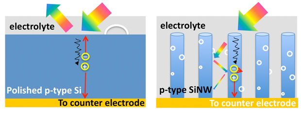
The trees’ vertical structure and branches are keys to capturing the maximum amount of solar energy, according to Wang. That’s because the vertical structure of trees grabs and adsorbs light while flat surfaces simply reflect it, Wang said, adding that it is also similar to retinal photoreceptor cells in the human eye. In images of Earth from space, light reflects off of flat surfaces such as the ocean or deserts, while forests appear darker.
Wang’s team has mimicked this structure in their “3D branched nanowire array” which uses a process called photoelectrochemical water-splitting to produce hydrogen gas. Water splitting refers to the process of separating water into oxygen and hydrogen in order to extract hydrogen gas to be used as fuel. This process uses clean energy with no green-house gas byproduct. By comparison, the current conventional way of producing hydrogen relies on electricity from fossil fuels

Schematic shows the light trapping effect in nanowire arrays. Photons on are bounced between single nanowires and eventually absorbed by them (R). By harvesting more sun light using the vertical nanotree structure, Wang’s team has developed a way to produce more hydrogen fuel efficiently compared to planar counterparts where they are reflected off the surface (L). Image Credit: Wang Research Group, UC San Diego Jacobs School of Engineering.
“Hydrogen is considered to be clean fuel compared to fossil fuel because there is no carbon emission, but the hydrogen currently used is not generated cleanly,” said Ke Sun, a PhD student in electrical engineering who led the project. 
By harvesting more sun light using the vertical nanotree structure, Wang’s team has developed a way to produce more hydrogen fuel efficiently compared to planar counterparts. Wang is also affiliated with the California Institute of Telecommunications and Information Technology and the Material Science and Engineering Program at UC San Diego.
The vertical branch structure also maximizes hydrogen gas output, said Sun. For example, on the flat wide surface of a pot of boiling water, bubbles must become large to come to the surface. In the nanotree structure, very small gas bubbles of hydrogen can be extracted much faster. “Moreover, with this structure, we have enhanced, by at least 400,000 times, the surface area for chemical reactions,” said Sun.

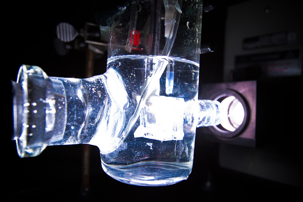
In this experiment, nanotree electrodes are submersed in water and illuminated by simulated sun light to measure electricity output of the device. Photo credit: Joshua Knoff, UC San Diego Jacobs School of Engineering.
In the long run, what Wang’s team is aiming for is even bigger: artificial photosynthesis. In photosynthesis, as plants absorb sunlight they also collect carbon dioxide (CO2) and water from the atmosphere to create carbohydrates to fuel their own growth. Wang’s team hopes to mimic this process to also capture CO2 from the atmosphere, reducing carbon emissions, and convert it into hydrocarbon fuel.
“We are trying to mimic what the plant does to convert sunlight to energy,” said Sun. “We are hoping in the near future our ‘nanotree’ structure can eventually be part of an efficient device that functions like a real tree for photosynthesis."
The team is also studying alternatives to zinc oxide, which absorbs the sun’s ultraviolet light, but has stability issues that affect the lifetime usage of the nanotree structure.