In a classic eureka moment, a team of physicists led by The City College of New York and including Herriot-Watt University and Corning Incorporated is showing how beams from ordinary laser pointers mimic quantum entanglement with the potential of doubling the data speed of laser communication.
Quantum entanglement is a phrase more likely to be heard on popular sci-fi television shows such as “Fringe” and “Doctor Who.” Described by Albert Einstein as “spooky action at a distance,” when two quantum things are entangled, if one is ‘touched’ the other will ‘feel it,’ even if separated by a great distance.
“At the heart of quantum entanglement is ‘nonseparability’ – two entangled things are described by an unfactorizable equation,” said City College PhD student Giovanni Milione. “Interestingly, a conventional laser beam (a laser pointer)’s shape and polarization can also be nonseparable.”
To make the laser beam’s shape and polarization nonseparable, the researchers transformed it into what Milione refers to as a vector beam – a polarization dependent shape. Then using off-the-shelf components to ‘touch’ only its polarization, they showed it could be encoded as two bits of information. Surprisingly, this was twice as much information that could be encoded as when the laser beam was separable.
“In principal, this could be used to double the data speed of laser communication,” said CCNY Distinguished Professor of Phyiscs Robert Alfano. “"While there’s no 'spooky action at a distance,' it's amazing that quantum entanglement aspects can be mimicked by something that simple."
An article on the experiment appears in the latest issue of the journal “Optics Letters” and was supported in part by the Army Research Office.
City College New York
The mission of the NWA is to globally promote nanotechnology solutions adoption across industries by connecting entrepreneurs with researchers, start-ups with investors, providers with potential customers, employers with job seekers, key players with one another, in an independent and mainly industry-oriented advocacy group – inclusive of business, academia, business-supporting associates, as well as affiliate government agencies and other associations.
Showing posts with label laser. Show all posts
Wednesday, October 28, 2015
Friday, October 23, 2015
Physicists create antimatter in record density
Positrons are plentiful in ultra-intense laser blasts
Physicists from Rice University and the University of Texas at Austin have found a new recipe for using intense lasers to create positrons — the antiparticle of electrons — in record numbers and density.
In a series of experiments described recently in the online journal Scientific Reports published by Nature, the researchers used UT’s Texas Petawatt Laser to make large number of positrons by blasting tiny gold and platinum targets.
Although the positrons were annihilated in a fraction of a microsecond, the experiments have implications for new realms of physics and astrophysics research, medical therapy and perhaps even space travel, said Rice physicist Edison Liang, lead author of the study.
“There are many futuristic technologies related to antimatter that people have been dreaming about for the last 50 years,” said Liang, the Andrew Hays Buchanan Professor of Astrophysics. “One is that antimatter is the most efficient form of energy storage. When antimatter annihilates with matter, it becomes pure energy. Nothing is left behind, unlike in fusion or fission or chemical-based reactions.”
With laser pulses as short as 130 femtoseconds (one femtosecond equals one-quadrillionth of a second), and peak intensity reaching almost 2 billion-trillion watts per square centimeter, the Texas Petawatt Laser is one of the world’s most intense short-pulse, high-energy lasers. In experiments that began in 2012, the Rice-UT team led by Liang completed more than 130 successful laser shots using gold and platinum targets.
“The physical conditions created in our experiments are more extreme than in previous experiments,” Liang said. “Antimatter has been created in accelerators for many decades, but the key difference here is that the laser pulses are very short and ultra intense. The density of antimatter created is high because it’s all concentrated in a tiny amount of space.”
In some shots, the team found they produced jets of particles that included about half as many positrons as electrons. Liang said a high ratio of positrons to electrons is important because physicists would like to produce a mixture that approaches a neutral “pair plasma” with equal numbers of positrons and electrons.
“Pair-dominated plasmas of positrons and electrons are fixtures in the universe,” he said. “They are believed to exist in the winds of pulsars, jets of quasars and gamma-ray bursts, and they are also thought to dominate the universe in the milliseconds following the Big Bang. We hope to use this laboratory platform to simulate some of those phenomena.”
Liang said the group would ultimately like to both create a dense pair-dominated plasma and find a way to capture it in a magnetic bottle for further study.
“Once you trap pure antimatter, the antiparticles can live a long time as long as they don’t touch any matter,” he said. “Since the 1950s, the Air Force, NASA and others have been talking about using antimatter for space travel. In space, weight is the key factor in determining how much fuel you can take with you.
Under the right conditions, positrons and electrons can pair up and orbit one another without touching or annihilating themselves. This paired arrangement, which behaves like a hydrogen atom with almost no mass, is known as positronium.
“But my main interest, which I’ve been concerned with for about 25 years, is to create a very high concentration of antimatter in a very small volume. We want to create a new form of quantum matter, a Bose-Einstein condensate (BEC), of antimatter. That is a really new domain of quantum physics that we could explore.”
A BEC is a collection of atoms or particles that are cooled to such low temperatures that their behavior is dictated by the laws of quantum mechanics. In a BEC, thousands of individual particles act collectively, marching in lock step as if they were a single entity.
“If we have a very large concentration of electrons and positrons, we could imagine making a BEC,” he said. “The beauty of positronium is that it is so light, it can actually become a BEC at relatively mild temperatures — about the temperature at which you would store liquid helium (minus 452 degrees Fahrenheit).”
The research is supported by the Department of Energy and the Rice University Faculty Initiative Fund.
Thursday, October 8, 2015
Laser-wielding physicists seize control of atoms’ behavior
Physicists have wondered in recent years if they could control how atoms interact using light. Now they know that they can, by demonstrating games of quantum billiards with unusual new rules.
In an article published online Oct. 5 in Physical Review Letters, a team of University of Chicago physicists explains how to tune a laser to make atoms attract or repel each other in an exotic state of matter called a Bose-Einstein condensate.
“This realizes a goal that has been pursued for the past 20 years,” said Cheng Chin, professor in physics, who led the team. “This exquisite control over interactions in a many-body system has great potential for the exploration of exotic quantum phenomena and engineering of novel quantum devices.
Many research groups in the United States and Europe have tried various ideas over the last decade. It was Logan Clark, a graduate student in Chin’s group, who came up with the first practical solution. He has now demonstrated the idea in the lab with cesium atoms chilled to temperatures just billionths of a degree above absolute zero, and the technique can be widely applied to other atomic species.
Clark compared the process to a billiards game, when one ball encounters another. “Normally, as soon as the surfaces touch, the balls repel each other and bounce away,” Clark said. In Chin’s lab, cesium atoms replace the billiard balls, and ordinarily they repel each other when they collide. But by turning up the laser while operating at a “magic” wavelength, Clark showed that the repulsion between atoms can be converted into attraction.
“The atoms exhibit fascinating behavior in this system,” he said. By exposing different parts of the sample to different laser intensities, “We can choose to make the atoms attract or repel each other, or pass right through each other without colliding.”
Alternatively, by oscillating their interactions, analogous to making the billiard balls rapidly grow and shrink while they roll, the atoms stick to each other in pairs.
The researchers explained two fundamental ways that lasers influence the atomic motion. One is to create potentials, like a bump or valley on the billiard table, proportional to laser intensity. The new way is to alter how billiard balls collide.
“We want our laser to control collisions, but we don’t want it to create any hills or valleys,” Clark said. When the laser is tuned to a “magic wavelength,” the beam creates no hills or valleys, but only affects collisions.
“This is because the magic wavelength happens to be in between two excited states of the atom, so they ‘magically’ cancel each other out,” he said.
Magic is a concept that has no place in science, though the word does enjoy fairly common use among atomic physicists. “Generally it is used to refer to a wavelength at which two effects cancel or are equal, in particular when this cancellation or equality is useful for some technological goal,” Clark said.
Laser spectroscopy of ultrathin semiconductor reveals rise of ‘trion’ quasiparticles
Insight into dynamics may spur improved materials for solar energy, quantum computing
Quasiparticles—excitations that behave collectively like particles—are central to energy applications but can be difficult to detect. Recently, however, researchers have seen evidence of quasiparticles called negative trions forming and fading in a layer of semiconducting material that is 100,000 times thinner than a human hair. Scientists at the Department of Energy’s Oak Ridge National Laboratory used ultrafast laser spectroscopy at the Center for Nanophase Materials Sciences (CNMS) to demystify the dynamics of the negative trions. They explored the behavior of the charged quasiparticle in a two-dimensional (2D) semiconductor that is an excellent absorber of sunlight.
Their insights, published in the journal Physical Review B, may prove important for advancing technologies for solar energy and quantum computing.
“We observed negative trions in a two-dimensional tungsten disulfide monolayer excited by a laser beam,” said ultrafast laser spectroscopist Abdelaziz Boulesbaa, who co-led the study with theorist Bing Huang and consulted with laser spectroscopy expert Alex Puretzky. “This discovery may open new opportunities to optoelectronic applications, including information technology, as well as fundamental research in the physics of low-dimensional materials.”
When a semiconductor absorbs light, electrons can be knocked loose and can participate in an electrical current. However, typically two charges form—one negative (an electron) and one positive (a hole)—and are bound to each other for a short time, traveling through the crystal as a quasiparticle called an “exciton.” When an exciton binds to an additional electron, the complex formed is a negative trion, or if it binds to an additional hole, the resulting quasiparticle is a positive trion.
Quasiparticles like excitons may sound exotic, but getting electrons and holes together is the basis for everyday light-emitting diodes (LEDs). When an electron and hole recombine in an LED, a photon is emitted. That’s the light we see in applications from traffic lights and electronic signage to camera flashes and vehicle headlights.
Whereas LEDs emit light, solar cells absorb light and convert its energy into electricity. To make solar cells work, scientists try to separate the electrons from the holes and collect those charges before they have a chance to recombine. Future materials may make use of negative trions to improve charge collection in solar cells, according to Boulesbaa.
Pump–probe experiment
To harness negative trions for improving solar cells and other optoelectronic technologies, scientists need answers to basic questions: How do negative trions form? How long do they live? Why do they form so efficiently in an ultrathin semiconductor?
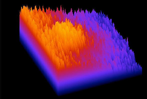
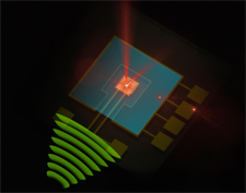
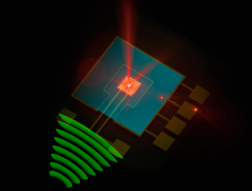
To answer these questions, the ORNL scientists needed a “camera” of sorts that could make a super-slow-motion movie to reveal quasiparticle dynamics, akin to the camera techniques photographers employ to capture speeding bullets obliterating apples—only a billion times faster. A split laser beam created that camera.
Employing half the laser beam, they fired laser pulses lasting a mere 40 femtoseconds (million-billionths of a second) to excite an ultrathin crystal of tungsten disulfide. Then, for their super slow-motion movie, they fashioned a strobe using the other half of the laser beam—an ultrafast flash of white light—and passed it through the crystal at different delayed times. By measuring the photon energy wavelengths (colors) the crystals absorbed at each time, the scientists built, frame by frame, a slow-motion “movie” of how trions form and fade. They probably skipped the popcorn, as their movie lasted only a nanosecond (one billionth of a second).
Their movie revealed trions form only after electron–hole pairs form. Then the holes get trapped, most likely by the substrate in contact with the crystal, leaving extra electrons.
These extra electrons allow the crystal to absorb another photon to form a negative trion. Because the ultrathin crystals are all “surface,” they have a lot of opportunity to interact with surroundings and to separate charges that are created, making them great trion generators.
Because the researchers used white light, a mixture of all frequencies of light in the visible spectrum, their observation of light of different colors revealed that two different trions had formed, which had not been seen previously.
Next the scientists will study the role of the substrate in defining optical and electrical properties of 2D semiconducting materials. Some substrates trap electrons, leaving excess holes to carry charges, whereas others trap holes, leaving excess electrons to carry charges. Furthermore, the researchers will isolate the 2D semiconductor from the substrate by introducing, in between, an insulator to prevent holes and electrons from reaching the substrate, allowing excitons to live longer and emit light for a greater duration.
The title of the paper is “Observation of two distinct negative trions in tungsten disulfide monolayers.” This research was conducted at the Center for Nanophase Materials Sciences at ORNL. Computations were performed at the National Energy Research Scientific Computing Center at Lawrence Berkeley National Laboratory. Both are DOE Office of Science User Facilities.
Monday, March 31, 2014
Never say never in the nano-world
![]() |
Artistic impressions of the nanoparticle in a laser trap. (Image credits: Iñaki Gonzalez and Jan Gieseler) |
An international team of researchers from Barcelona, Zurich and Vienna found that a nanoparticle trapped with laser light temporarily violates the famous second law of thermodynamics, something that is impossible on human time and length scale. They report about their results in the latest issue of the prestigious scientific journal Nature Nanotechnology.
Surprises at the nanoscale
Watching a movie played in reverse often makes us laugh because unexpected and mysterious things seem to happen: glass shards lying on the floor slowly start to move towards each other, magically assemble and suddenly an intact glass jumps on the table where it gently gets to a halt. Or snow starts to from a water puddle in the sun, steadily growing until an entire snowman appears as if molded by an invisible hand. When we see such scenes, we immediately realize that according to our everyday experience something is out of the ordinary. Indeed, there are many processes in nature that can never be reversed. The physical law that captures this behavior is the celebrated second law of thermodynamics, which posits that the entropy of a system – a measure for the disorder of a system – never decreases spontaneously, thus favoring disorder (high entropy) over order (low entropy).
However, when we zoom into the microscopic world of atoms and molecules, this law softens up and looses its absolute strictness. Indeed, at the nanoscale the second law can be fleetingly violated. On rare occasions, one may observe events that never happen on the macroscopic scale such as, for example heat transfer from cold to hot which is unheard of in our daily lives. Although on average the second law of thermodynamics remains valid even in nanoscale systems, scientists are intrigued by these rare events and are investigating the meaning of irreversibility at the nanoscale.
Nanoparticles in laser traps
Recently, a team of physicists of the University of Vienna, the Institute of Photonic Sciences in Barcelona and the Swiss Federal Institute of Technology in Zürich succeeded in accurately predicting the likelihood of events transiently violating the second law of thermodynamics. They immediately put the mathematical fluctuation theorem they derived to the test using a tiny glass sphere with a diameter of less than 100 nm levitated in a trap of laser light. Their experimental set-up allowed the research team to capture the nano-sphere and hold it in place, and, furthermore, to measure its position in all three spatial directions with exquisite precision. In the trap, the nano-sphere rattles around due to collisions with surrounding gas molecules.
By a clever manipulation of the laser trap the scientists cooled the nano-sphere below the temperature of the surrounding gas and, thereby, put it into a non-equilibrium state. They then turned off the cooling and watched the particle relaxing to the higher temperature through energy transfer from the gas molecules. The researchers observed that the tiny glass sphere sometimes, although rarely, does not behave as one would expect according to the second law: the nano-sphere effectively releases heat to the hotter surroundings rather than absorbing the heat. The theory derived by the researchers to analyze the experiment confirms the emerging picture on the limitations of the second law on the nanoscale.
Nanomachines out of equilibrium
The experimental and theoretical framework presented by the international research team in the renowned scientific journal Nature Nanotechnology has a wide range of applications. Objects with sizes in the nanometer range, such as the molecular building blocks of living cells or nanotechnological devices, are continuously exposed to a random buffeting due to the thermal motion of the molecules around them. As miniaturization proceeds to smaller and smaller scales nanomachines will experience increasingly random conditions. Further studies will be carried out to illuminate the fundamental physics of nanoscale systems out of equilibrium. The planned research will be fundamental to help us understand how nanomachines perform under these fluctuating conditions.
Original publication in Nature Nanotechnology
Dynamic Relaxation of a Levitated Nanoparticle from a Non-Equilibrium Steady State. Jan Gieseler, Romain Quidant, Christoph Dellago, and Lukas Novotny. Nature Nanotechnology AOP, February 28, 2014. DOI: 10.1038/NNANO.2014.40
Source: http://medienportal.univie.ac.at//presse/aktuelle-pressemeldungen/detailansicht/artikel/never-say-never-in-the-nano-world/
Thursday, March 6, 2014
Ultra sensitive detection of radio waves with lasers

The method, called optomechanics, is a complex interaction between a mechanical movement and optical radiation. The laser light has almost no noise, as all its photons are identical. In this way, the special properties of the nanomembrane are fully exploited. (Artists impression by Mette Høst)
‘Noise’ in the detector of a measuring instrument is first and foremost due to heat, that causes atoms and electrons to move chaotically, so the measurements become imprecise. The usual method to reduce noise in the detector of the measuring equipment is therefore to cool it down to 5-10 degrees Kelvin, which corresponds to approx. minus 265 degrees C. This is expensive and stille does not allow to measure the weakest signals.
“We have developed a detector that does not need to be cooled down, but which can operate at room temperature and yet hardly has any thermal noise. The only noise that fundamentally remains is so-called quantum noise, which is the minimal fluctuations of the laser light itself,” explains Eugene Polzik, Professor and Head of the research center Quantop at the Niels Bohr Institute at the University of Copenhagen.
Optomechanical method
The method, called optomechanics, is a complex interaction between a mechanical movement and optical radiation.
The experiment consists of an antenna, which picks up the radio waves, a capacitor and a laser beam. The antenna picks up the radio waves and transfers the signal to the capacitor, which is read by the laser beam - that is to say the capacitor and the laser beam make up the detector. But the capacitor is not an ordinary pair of metal plates.

The nanomembrane itself is made of silicon nitrate and is coated with a thin layer of aluminum, since there has to be a metallic substance to better interact with the electric field. The membrane is separated from the surroundings by being enclosed in a vacuum chamber so that it responds as if it had been cooled down to two degrees Kelvin (minus 271 C).
“In our system, one metal plate in the capacitor is replaced by a 50 nanometer thick membrane (a nanometer is a millionth of a millimeter). It is this nanomembrane that allows us to make ultrasensitive measurements without cooling the system, explains Research Assistant Professor Albert Schliesser, who has coordinated the the experiments in Quantop’s optomechanical laboratory at the Niels Bohr Institute.
He explains that the capacitor is made up of three layers. At the bottom is a chip made of glass with a layer of aluminum, where the positive and negative poles are. The nanomembrane itself is made of silicon nitrate and is coated with a thin layer of aluminum, since there has to be a metallic substance to better interact with the electric field. The chip and the membrane are only separated by a micrometer.
The radio wave signal produces fluctuations in the membrane and you can now read the signal optically using a laser beam. This is done through a complex interaction between the membrane’s mechanical fluctuations, the electrical properties of the metallic layer and the light that is hitting the membrane.

The experiments are carried out here at the Quantop laboratories at the Niels Bohr Institute. The research group consists of Research Assistant Professor Albert Schliesser, PhD students Tolga Bagci and Anders Simonsen and Professor Eugene Polzik.
The method was developed by Eugene Polzik and Albert Schliesser in collaboration with the theoretical quantum optics groups at the Niels Bohr Institute and the Joint Quantum Institute in Maryland, USA. The electromechanical chip was developed at Nanotech, DTU.
Ultrasensitive measurements
This optomechanical method has three types of noise: Electrical noise in the antenna, mechanical thermal noise in the membrane and quantum noise of the light. The electrical noise is technical and is mostly due to disturbances from the environment.
“This has been a technical challenge and the two PhD students Tolga Bagci and Anders Simonsen have worked days and nights to solve the problem. The solution has been to find just the right way to shield the experiment,” says Albert Schliesser.

The two PhD students Tolga Bagci and Anders Simonsen have worked days and nights to solve the problem with noise due to disturbances from the environment. The solution has been to find just the right way to shield the experiment.
Everything takes place at normal room temperature and yet there is almost no mechanical ‘thermal noise’. This is surprising and is due to several factors - including the membrane’s extremely high mechanical properties and that the membrane is separated from the surroundings by being enclosed in a vacuum chamber so that it responds as if it had been cooled down to two degrees Kelvin (minus 271 C).
The laser light has almost no noise, as all its photons are identical. In this way, the special properties of the nanomembrane are fully exploited.
Groundbreaking method
“This membrane is an extremely good oscillator and that is why it is so ultrasensitive. At room temperature, it works as effectively as if it was cooled down to minus 271 C and we are working to get it even closer to minus 273 degrees C, which is the absolute minimum. In addition, it is a huge advantage to use optical detection, as instead of using ordinary copper wires to transmit the signal, you can use fiber optic cables, where there is no energy loss,” explains Eugene Polzik.

The method was developed by Eugene Polzik and Albert Schliesser in collaboration with the theoretical quantum optics groups at the Niels Bohr Institute and the Joint Quantum Institute in Maryland, USA.
This is a groundbreaking new method for measuring electrical signals that could have a significant impact on future technologies. Eugene Polzik and Albert Schliesser see great potential in the new super sensitive method, both in equipment for medical treatment and for observations in space, where cosmologists measure radio radiation in order to study the infancy of the universe.
Source: http://www.nbi.ku.dk/english/news/news14/ultra-sensitive-detection-of-radio-waves-with-lasers/Tuesday, December 17, 2013
Ultrafast heating of water - This pot boils faster than you can watch it
A single terahertz flash can heat the water cloud to 600 degrees centigrade, while leaving all water molecules intact. Credit: Oriol Vendrell/DESY |

Novel method opens new paths for experiments with heated samples of biological relevance
Scientists from the Hamburg Center for Free-Electron Laser Science have devised a novel way to boil water in less than a trillionth of a second. The theoretical concept, which has not yet been demonstrated in practice, could heat a small amount of water by as much as 600 degrees Celsius in just half a picosecond (a trillionth of a second).
That is much less than the proverbial blink of an eye: one picosecond is to a second what one second is to almost 32 millennia.
This would make the technique the fastest water-heating method on earth.
The novel concept opens up interesting new ways for experiments with heated samples of chemical or biological relevance, as the inventors report in this week's issue of the scientific journal Angewandte Chemie - International Edition (Nr. 51, 16 December). "Water is the single most important medium in which chemical and biological processes take place," explains DESY scientist Dr. Oriol Vendrell from the Center for Free-Electron Laser Science CFEL, a cooperation of DESY, the University of Hamburg and the German Max Planck Society. "Water is not just a passive solvent, but plays an important role in the dynamics of biological and chemical processes by stabilising certain chemical compounds and enabling specific reactions."
All it takes for superfast water heating is a concentrated flash of terahertz radiation. Terahertz radiation consists of electromagnetic waves with a frequency between radio waves and infrared. Terahertz flashes can be generated with devices called free-electron lasers that send accelerated electrons on a well defined slalom course. The particles emit electromagnetic waves in each bend that add up to an intense laser like pulse. The terahertz pulse changes the strength of the interaction between water molecules in a very short time, which immediately start to vibrate violently.
The scientists calculated the interaction of the terahertz flash with bulk water. The simulations were performed at the Supercomputer Center Jülich and used a total of 200,000 hours of processor time by massively parallel computing. On a single processor machine this would correspond to about 20 years of computation. "We have calculated that it should be possible to heat up the liquid to about 600 degrees Celsius within just half a picosecond, obtaining a transiently hot and structureless environment still at the density of the liquid, leaving all water molecules intact," explains Vendrell.
The novel method can only heat about one nanolitre (billionth of a litre) in one go. This may sound small, but is large enough for most experiments. For comparison, ink-jet printers fire droplets that are as small as one picolitre, which is a thousand times less than a nanolitre.
"The idea is to heat-up the 'solvent' so that many molecules start the desired chemical process at the same time and then watch the reaction evolve," explains Vendrell, who worked out the super heater with co-authors Pankaj Kr. Mishra and Prof. Robin Santra, also of CFEL. Although the hot mini-cloud will fly apart in less than a millisecond (a thousandth of a second), it lasts long enough to unravel everything of interest in thermal reactions such as the combination of small organic molecules to form new substances. The team currently investigates how the intense pulse of terahertz radiation affects different types of molecules dissolved in water, from inorganic to biological systems.
The reaction progress can be probed with ultrashort X-ray flashes like they will be produced by the 3.4-kilometre-long X-ray free-electron laser European XFEL, which currently is being built between the DESY campus in Hamburg and the neighbouring town of Schenefeld. When completed, the European XFEL will be able to generate 27,000 intense X-ray laser flashes per second, which can for example be used to record the different stages of chemical reactions.
One advantage of the heating method is that the terahertz pulse can be very well synchronised with the X-ray flashes to start the experiment and then probe the reaction after a well defined time. "The transient and hot environment achieved by the terahertz pulse could have interesting properties, like a matrix to study activated chemical processes," says Vendrell. "This will be the subject of further investigations."
Monday, December 9, 2013
Laser light at useful wavelengths from semiconductor nanowires
Thread-like semiconductor structures called nanowires, so thin that they are effectively one-dimensional, show potential as lasers for applications in computing, communications, and sensing.
Scientists at the Technische Universität München (TUM) have demonstrated laser action in semiconductor nanowires that emit light at technologically useful wavelengths and operate at room temperature. They now have documented this breakthrough in the journal Nature Communications and, in Nano Letters, have disclosed further results showing enhanced optical and electronic performance.
"Nanowire lasers could represent the next step in the development of smaller, faster, more energy-efficient sources of light," says Prof. Jonathan Finley, director of TUM's Walter Schottky Institute. Potential applications include on-chip optical interconnects or even optical transistors to speed up computers, integrated optoelectronics for fiber-optic communications, and laser arrays with steerable beams. "But nanowires are also a bit special," Finley adds, "in that they are very sensitive to their surroundings, have a large surface-to-volume ratio, and are small enough, for example, to poke into a biological cell." Thus nanowire lasers could also prove useful in environmental and biological sensing.
These experimental nanowire lasers emit light in the near-infrared, approaching the "sweet spot" for fiber-optic communications. They can be grown directly on silicon, presenting opportunities for integrated photonics and optoelectronics. And they operate at room temperature, a prerequisite for real-world applications.
Tailored in the lab, with an eye toward industry
Tiny as they are – a hundred to a thousand times thinner than a human hair – the nanowire lasers demonstrated at TUM have a complex "core-shell" cross-section with a profile of differing semiconductor materials tailored virtually atom by atom.
The nanowires' tailored core-shell structure enables them to act both as lasers, generating coherent pulses of light, and as waveguides, similar to optical fibers. Like conventional communication lasers, these nanowires are made of so-called III-V semiconductors, materials with the right "bandgap" to emit light in the near-infrared. A unique advantage, Finley explains, is that the nanowire geometry is "more forgiving than bulk crystals or films, allowing you to combine materials that you normally can't combine." Because the nanowires arise from a base only tens to hundreds of nanometers in diameter, they can be grown directly on silicon chips in a way that alleviates restrictions due to crystal lattice mismatch – thus yielding high-quality material with the potential for high performance.
Put these characteristics together, and it becomes possible to imagine a path from applied research to a variety of future applications. A number of significant challenges remain, however. For example, laser emission from the TUM nanowires was stimulated by light – as were the nanowire lasers reported almost simultaneously by a team at the Australian National University – yet practical applications are likely to require electrically injected devices.
Nanowire lasers: a technological frontier with bright prospects
The newly published results are largely due to a team of scientists who are beginning their careers, under the guidance of Dr. Gregor Koblmüller and other senior researchers, at the frontier of a new field. Doctoral candidates including Benedikt Mayer, Daniel Rudolph, Stefanie Morkötter and Julian Treu combined their efforts, working together on photonic design, material growth, and characterization using electron microscopy with atomic resolution.
Ongoing research is directed toward better understanding the physical phenomena at work in such devices as well as toward creating electrically injected nanowire lasers, optimizing their performance, and integrating them with platforms for silicon photonics.
"At present very few labs in the world have the capability to grow nanowire materials and devices with the precision required," says co-author Prof. Gerhard Abstreiter, founder of the Walter Schottky Institute and director of the TUM Institute for Advanced Study. "And yet," he explains, "our processes and designs are compatible with industrial production methods for computing and communications. Experience shows that today's hero experiment can become tomorrow's commercial technology, and often does."
This research was supported in part by the German Excellence Initiative through the TUM Institute for Advanced Study and the Excellence Cluster Nanosystems Initiative Munich (NIM); by the German Research Foundation (DFG) through Collaborative Research Center SFB 631; by the European Union through a Marie Curie European Reintegration Grant, the QUROPE project SOLID, and the EU-MC network INDEX; by a CINECA award under the ISCRA initiative; and by a grant from Generalitat Valenciana.
Source: http://www.tum.de/en/about-tum/news/press-releases/short/article/31226/
Subscribe to:
Posts (Atom)