Showing posts with label nanocrystals. Show all posts

Monday, November 30, 2015

Researchers Find New Phase of Carbon, Make Diamond at Room Temperature


Researchers from North Carolina State University have discovered a new phase of solid carbon, called Q-carbon, which is distinct from the known phases of graphite and diamond. They have also developed a technique for using Q-carbon to make diamond-related structures at room temperature and at ambient atmospheric pressure in air.

Phases are distinct forms of the same material. Graphite is one of the solid phases of carbon; diamond is another.

“We’ve now created a third solid phase of carbon,” says Jay Narayan, the John C. Fan Distinguished Chair Professor of Materials Science and Engineering at NC State and lead author of three papers describing the work. “The only place it may be found in the natural world would be possibly in the core of some planets.”

Q-carbon has some unusual characteristics. For one thing, it is ferromagnetic – which other solid forms of carbon are not.

“We didn’t even think that was possible,” Narayan says.
In addition, Q-carbon is harder than diamond, and glows when exposed to even low levels of energy.

“Q-carbon’s strength and low work-function – its willingness to release electrons – make it very promising for developing new electronic display technologies,” Narayan says.

But Q-carbon can also be used to create a variety of single-crystal diamond objects. To understand that, you have to understand the process for creating Q-carbon.

Researchers start with a substrate, such as such as sapphire, glass or a plastic polymer. The substrate is then coated with amorphous carbon – elemental carbon that, unlike graphite or diamond, does not have a regular, well-defined crystalline structure. The carbon is then hit with a single laser pulse lasting approximately 200 nanoseconds. During this pulse, the temperature of the carbon is raised to 4,000 Kelvin (or around 3,727 degrees Celsius) and then rapidly cooled.

This operation takes place at one atmosphere – the same pressure as the surrounding air.
The end result is a film of Q-carbon, and researchers can control the process to make films between 20 nanometers and 500 nanometers thick.

By using different substrates and changing the duration of the laser pulse, the researchers can also control how quickly the carbon cools. By changing the rate of cooling, they are able to create diamond structures within the Q-carbon.

“We can create diamond nanoneedles or microneedles, nanodots, or large-area diamond films, with applications for drug delivery, industrial processes and for creating high-temperature switches and power electronics,” Narayan says. “These diamond objects have a single-crystalline structure, making them stronger than polycrystalline materials. And it is all done at room temperature and at ambient atmosphere – we’re basically using a laser like the ones used for laser eye surgery. So, not only does this allow us to develop new applications, but the process itself is relatively inexpensive.”

And, if researchers want to convert more of the Q-carbon to diamond, they can simply repeat the laser-pulse/cooling process.

If Q-carbon is harder than diamond, why would someone want to make diamond nanodots instead of Q-carbon ones? Because we still have a lot to learn about this new material.

“We can make Q-carbon films, and we’re learning its properties, but we are still in the early stages of understanding how to manipulate it,” Narayan says. “We know a lot about diamond, so we can make diamond nanodots. We don’t yet know how to make Q-carbon nanodots or microneedles. That’s something we’re working on.”

NC State has filed two provisional patents on the Q-carbon and diamond creation techniques.

Tuesday, September 29, 2015

Computing A Textbook of Crystal Physics

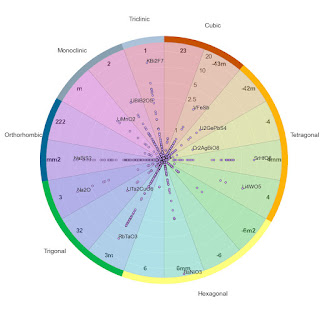
Berkeley Lab scientists publish world’s largest database of piezoelectric properties


Disturbing a material’s crystal lattice can create a charge imbalance that leads to a voltage across the material. This phenomena, called the “piezoelectric effect,” was first demonstrated in 1880 by Jacques and Pierre Curie in materials such as quartz, topaz and Rochelle salt. Today, piezoelectricity is recognized as a valuable property and the market for piezoelectric materials is rapidly expanding with applications that encompass a variety of technologies, ranging from medical imaging to sonar to energy harvesting.
Despite its rising technological importance, the piezoelectric effect has been measured in only a handful of materials, but this is about to change. Researchers at Berkeley Lab and the University of California (UC) Berkeley have developed a methodology that enabled them to compute piezoelectric constants for nearly 1,000 inorganic compounds.
“People know how to calculate piezoelectric tensors but now we’ve developed a robust workflow for these calculations, which provides an unprecedented scaling of methodology for testing materials,” says Kristin Persson, staff scientist at Berkeley Lab’s Materials Sciences Division and leader of the Materials Project, which provides open web-based access to computed information on known and predicted materials. “Not only does this provide new open-access data to the community, but also indicates what structures and elements might be important for developing novel materials with strong piezoelectric properties.”
Kristin Persson leads the Materials Project, which provides open web-based access to computed information on known and predicted materials. (Photo by Roy Kaltschmidt)
In the new high-throughput calculations using the computing resources at the National Energy Research Scientific Computing Center (NERSC), hundreds of structures can be computed simultaneously. Compared to conventional experimental measurements, which could take years to cover the same number of materials, the “computational characterization” quickly identifies promising inorganic compounds in the Materials Project database that have the possibility of exhibiting piezoelectric behavior.
Persson, along with Mark Asta, staff scientist at Berkeley Lab and professor in UC Berkeley’s Department of Materials Science and Engineering, are co-authors of a paper describing this research in the journal Scientific Data. The paper is titled “A database to enable discovery and design of piezoelectric materials.” The other authors are Maarten de Jong, Wei Chen and   Henry Geerlings.
Certain structures of elements give rise to large piezoelectric responses: when subjected to a stress, they develop a stronger electric field. The larger the response – indicated by the tensor – the better the piezoelectric performance.
“The new database …will be invaluable for guiding the discovery of new candidate materials featuring enhanced performance, lower cost, and or more environmentally friendly constituents,” Asta says.
“We don’t collect experimental data – but we compare calculations with reported experimental piezoelectric constants,” says Persson. “For new materials that have not been measured before, it’s up to the community to test the data – by growing a film or a single crystal – and comparing with Materials Project computations.”
In 1910, Woldemar Voigt published the Textbook on Crystal Physics, defining the piezoelectric constants of 20 natural crystal classes. Now, the Materials Project has published tensor analyses that suggest completely new materials as potential piezoelectrics.
“The highest performing piezoelectric ceramics currently available contain high concentrations of lead, and significant efforts are aimed at identifying new lead-free compounds,” Asta says. “The new database is anticipated to greatly accelerate such materials discovery efforts.”
This research was funded by the Materials Project Center and made use of resources of the National Energy Research Scientific Computing Center (NERSC), supported by the Office of Basic Energy Sciences of the US Department of Energy.

Thursday, September 24, 2015

Designed defects in liquid crystals can guide construction of nanomaterials


Imperfections running through liquid crystals can be used as miniscule tubing, channeling molecules into specific positions to form new materials and nanoscale structures, according to engineers at the University of Wisconsin-Madison. The discovery could have applications in fields as diverse as electronics and medicine.
"By controlling the geometry of the system, we can send these channels from any one point to any other point," says Nicholas Abbott, a UW-Madison professor of chemical and biological engineering. "It's quite a versatile approach."
Photo: Nicholas Abbott
Nicholas Abbott
So far, Abbott and his collaborators at UW-Madison's Materials Research Science and Engineering Center (MRSEC) have been able to assemble phospholipids — molecules that can organize into layers in the walls of living cells — within liquid crystal defects.
Their technique may also be useful for assembling metallic wires and various semiconducting structures vital to electronics. There's also potential for mimicking the selective abilities of a membrane, designing a defect so that one type of molecule can pass through while others can't.
"This is an enabling discovery," Abbott says. "We're not looking for a specific application, but we're showing a versatile method of fabrication that can lead to structures you can't make any other way."
The researchers — including UW-Madison graduate students Xiaoguang Wang, Daniel S. Miller and Emre Bukusoglu, and Juan J. de Pablo, a former UW-Madison engineering professor now at the University of Chicago — published details of their advance this week in the journal Nature Materials.
For about 20 years, Abbott's research has examined the surfaces of soft materials, including liquid crystals — a particular phase of matter in which liquid-like materials also exhibit some of the molecular organization of solids.
"We've done a lot of work in the past at the interfaces of liquid crystals, but we're now looking inside the liquid crystal," he says. "We're looking at how to use the internal structure of liquid crystals to direct the organization of molecules. There's no prior example of using a defect in a liquid crystal to template molecular organization."
When the researchers manipulate the geometry of a liquid crystalline system, a variety of different defects can result. Abbott's group assembled liquid crystals with defects shaped like ropes or lines they call "disclinations," that formed templates they could fill with amphiphilic (water- and fat-loving) molecules.
Then they can link together assemblies of molecules and remove the liquid crystal templates, leaving behind the amphiphilic building blocks in a lasting, nanoscale structure.
The research is an example of how liquid crystal research is taking us from the nano to macro world, says Dan Finotello, program director at the National Science Foundation, which funds the MRSEC.
"It is also an exquisite demonstration of MRSEC programs' high impact," Finotello says. "MRSECs bring together several researchers of varied experience and complementary expertise who are then able to advance science at a considerably faster rate."

Thursday, September 10, 2015

UT researchers give nanosheets local magnetic properties


Two-dimensional crystals are very suitable for creating high-quality magnetic thin films. This appears from two recent publications written by scientists from the University of Twente's MESA+ research institute. The researchers show that by growing the magnetic layers on various 2D crystals, better known as nanosheets, you can control the preferred direction of the magnetism very locally.

In an article published in Advanced Functional Materials, they present this method to create magnetic patterns on the micrometer scale. In Angewandte Chemie, they demonstrate that you can make the nanosheets in less than a minute, while the synthesis process had been known to be very slow. The magnetic films can be deployed for many different applications, such as new generations of smartphones.

With pulsed laser deposition (PLD) you can achieve controlled growth of thin layers of certain materials. Here, a material is heated rapidly with a powerful laser beam, so that it evaporates and a plasma is created. This spreads quickly in a vacuum chamber and is deposited on a substrate where it forms a thin layer. In this way you can control the thickness of the layer and you can form smooth and thin layers, often with special properties that are interesting for use in electronics and electro-mechanics, for example. For such applications, it is however essential that you can also make patterns in the layered materials. This is not easy, especially because the substrate needs to be heated to temperatures above 500° C during the PLD process. Many of the existing methods are therefore not adapted to existing manufacturing methods for microstructures.

Use of nanosheets

The UT researchers have now developed a new method, in which they make use of nanosheets obtained from three-dimensional crystals with a layered structure. If you dissolve these crystals in a special liquid, they spontaneously disintegrate into individual nanosheets. It was long thought that the crystal disintegration process could take weeks. However, the researchers have now shown that the nanosheets are already able to form within a few seconds, which opens the way for the production of nanosheets on a large scale.

Based on the solution, various nanosheets can be introduced in micro-patterns on a substrate. These patterns form the starting point for the growth of thin magnetic layers of magnetic LaSrMnO3 at high temperatures by means of PLD. Depending on the type of nanosheet the structure of the magnetic film assumes a specific orientation, and thus determines the magnetism of the film at that location. The process is monitored by means of, for example, electron backscatter diffraction (EBSD); a technique that makes it possible to 'reveal' the structure in the patterns.


Caption: EBSD image showing the local structure of a thin film. The left half of these images shows the preferred direction of the LaSrMnO3-film perpendicular to the growth direction, while the right half shows the directions in the plane with the contours of the individual nanosheets clearly visible. The distance between two lines in the pattern is a few micrometers.

FUNCTIONAL PROPERTIES

The researchers show that you can use the micro patterns to control the functional properties of a material in detail. In addition to magnetism, it is possible to pattern other properties at the micrometer scale. An important step has thus been taking in bridging the gap between scientific research into artificial layered crystals and their ultimate application. The group from Twente plays a leading role in this worldwide. 


RESEARCH

The research was performed by scientists from the Inorganic Materials Science department of UT research institute MESA+. It forms part of the TOP project funded by the Netherlands Organisation for Scientific Research (NWO) and the Chinese Scholarship Council. The research involved close cooperation with the Condensed-Matter and Medical Physics group at the University of California (UC, Irvine). 


University of Twenty

Tuesday, May 13, 2014

A new quantum memory on the horizon

Memory candidate with a bright future: Max Planck
researchers have addressed individual praseodymium
ions in the crystal of an yttrium orthosilicate using
resourceful microscopy and laser technologies.
This opens up the possibility of storing quantum
information in these ions, which have several advantages
compared to other memory candidates.
© MPI for the Science of Light
Sensitive measurements can be used to detect signals from an individual ion in a crystal

A promising material is lining itself up as a candidate for a quantum memory. A team at the Max Planck Institute for the Science of Light in Erlangen is the first to succeed in performing high-resolution spectroscopy and microscopy on individual rare earth ions in a crystal. With the aid of ingenious laser and microscopy technology they determined the position of triply charged positive praseodymium atoms (Pr3+) in an yttrium orthosilicate to within a few nanometres and investigated their weak interaction with light. In addition to its impact on fundamental studies, the work may make an important contribution to the quantum computers of the future because the ions investigated are suitable for storing and processing quantum information.

Around the globe, numerous researchers are working on components for the quantum computers of the future, which will be able to process information significantly faster than today. The key elements of these super-computers include quantum systems with optical properties similar to those of an atom. This is why many researchers are currently focusing their attention on different systems such as light-emitting crystal defects (“colour centres”) in diamond or on semiconductor quantum dots. However, so far there has been no ideal solution. “Some of the light sources lose their brightness or flicker in an uncontrollable way,” explains Vahid Sandoghdar, who heads the Nano-Optics Department at the Max Planck Institute for the Science of Light in Erlangen. “Others are greatly affected by the environment into which they are embedded.”

Researchers observe the signals of an individual ion

It has long been known that the rare earth ions such as neodymium or erbium do not suffer from these problems – which is also why they play a key role in lasers or laser amplifiers. They emit only weakly, however, and are therefore difficult to detect. This is precisely what Tobias Utikal, Emanuel Eichhammer and Stephan Götzinger from Sandoghdar’s Group in Erlangen have succeeded to do: after more than six years of intensive research they were able to detect individual praseodymium ions, pinpoint them with an accuracy of a few nanometres, and measure their optical properties with an accuracy never achieved before.
The triply charged, positive ions were embedded in tiny microcrystals and nanocrystals of yttrium orthosilicate (YSO). Their energies varied only slightly depending on their position in the crystal. In other words, they reacted to slightly different frequencies. The scientists used this to excite individual ions in the crystals with a laser and to observe how they emit the energy after some time in form of light. “Because rare earth ions are not strongly affected by the thermal and acoustic oscillations of the crystal, some of their energy states are unusually stable,” says Sandoghdar. “It takes more than a minute before they make the transition into the ground state again – a million times longer than for most of the other quantum systems that have been investigated so far.”
The aim is for the signals of the ions to be even easier to observe in the future. Since an individual ion responds with less than 100 photons per second at the moment, the Erlangen-based scientists want to employ nano-antennas and microcavities to amplify the praseodymium signal by a hundred or a thousand times.

http://www.mpg.de/8202685/quantum-ion-crystal

Thursday, December 19, 2013

Liquid Crystal 'Flowers' That Can Be Used as Lenses

A team of material scientists, chemical engineers and physicists from the University of Pennsylvania has made another advance in their effort to use liquid crystals as a medium for assembling structures.
In their earlier studies, the team produced patterns of “defects,” useful disruptions in the repeating patterns found in liquid crystals, in nanoscale grids and rings. The new study adds a more complex pattern out of an even simpler template: a three-dimensional array in the shape of a flower.      
And because the petals of this “flower” are made of transparent liquid crystal and radiate out in a circle from a central point, the ensemble resembles a compound eye and can thus be used as a lens.  
The team consists of Randall Kamien, professor in the School of Arts and Sciences’ Department of Physics and Astronomy; Kathleen Stebe, the School of Engineering and Applied Science’s deputy dean for research and professor in Chemical and Biomolecular Engineering and Shu Yang, professor in Engineering’s departments of Materials Science and Engineering and Chemical and Biomolecular Engineering. Members of their labs also contributed to the new study, including lead author Daniel Beller, Mohamed Gharbi and Apiradee Honglawan.    
Their work was published in Physical Review X.   
The researchers’ ongoing work with liquid crystals is an example of a growing field of nanotechnology known as “directed assembly,” in which scientists and engineers aim to manufacture structures on the smallest scales without having to individually manipulate each component. Rather, they set out precisely defined starting conditions and let the physics and chemistry that govern those components do the rest.  
The starting conditions in the researchers previous experiments were templates consisting of tiny posts. In one of their studies, they showed that changing the size, shape or spacing of these posts would result in corresponding changes in the patterns of defects on the surface of the liquid crystal resting on top of them. In another experiment, they showed they could make a “hula hoop” of defects around individual posts, which would then act as a second template for a ring of defects at the surface.
In their latest work, the researchers used a much simpler cue.    
“Before we were growing these liquid crystals on something like a trellis, a template with precisely ordered features,” Kamien said. “Here, we’re just planting a seed.”
The seed, in this case, were silica beads — essentially, polished grains of sand. Planted at the top of a pool of liquid crystal flower-like patterns of defects grow around each bead.
The key difference between the template in this experiment and ones in the research team’s earlier work was the shape of the interface between the template and the liquid crystal.
In their experiment that generated grid patterns of defects, those patterns stemmed from cues generated by the templates’ microposts. Domains of elastic energy originated on the flat tops and edges of these posts and travelled up the liquid crystal’s layers, culminating in defects. Using a bead instead of a post, as the researchers did in their latest experiment, makes it so that the interface is no longer flat.             
“Not only is the interface at an angle, it’s an angle that keeps changing,” Kamien said. “The way the liquid crystal responds to that is that it makes these petal-like shapes at smaller and smaller sizes, trying to match the angle of the bead until everything is flat.”
Surface tension on the bead also makes it so these petals are arranged in a tiered, convex fashion. And because the liquid crystal can interact with light, the entire assembly can function as a lens, focusing light to a point underneath the bead.
“It’s like an insect’s compound eye, or the mirrors on the biggest telescopes,” said Kamien. “As we learn more about these systems, we’re going to be able to make these kinds of lenses to order and use them to direct light.”
This type of directed assembly could be useful in making optical switches and in other applications.
The research was supported by the National Science Foundation, Penn’s Materials Science Research and Engineering Center and the Simons Foundation.

Wednesday, November 27, 2013

Slowly cooled DNA transforms disordered nanoparticles into orderly crystal

Nature builds flawless diamonds, sapphires and other gems. Now a Northwestern University research team is the first to build near-perfect single crystals out of nanoparticles and DNA, using the same structure favored by nature.
“Single crystals are the backbone of many things we rely on -- diamonds for beauty as well as industrial applications, sapphires for lasers and silicon for electronics,” said nanoscientist Chad A. Mirkin. “The precise placement of atoms within a well-defined lattice defines these high-quality crystals.
“Now we can do the same with nanomaterials and DNA, the blueprint of life,” Mirkin said. “Our method could lead to novel technologies and even enable new industries, much as the ability to grow silicon in perfect crystalline arrangements made possible the multibillion-dollar semiconductor industry.”
His research group developed the “recipe” for using nanomaterials as atoms, DNA as bonds and a little heat to form tiny crystals. This single-crystal recipe builds on superlattice techniques Mirkin’s lab has been developing for nearly two decades.
In this recent work, Mirkin, an experimentalist, teamed up with Monica Olvera de la Cruz, a theoretician, to evaluate the new technique and develop an understanding of it. Given a set of nanoparticles and a specific type of DNA, Olvera de la Cruz showed they can accurately predict the 3-D structure, or crystal shape, into which the disordered components will self-assemble. 
Mirkin is the George B. Rathmann Professor of Chemistry in the Weinberg College of Arts and Sciences. Olvera de la Cruz is a Lawyer Taylor Professor and professor of materials science and engineering in the McCormick School of Engineering and Applied Science. The two are senior co-authors of the study.
The results will be published Nov. 27 in the journal Nature
Chad Mirkin
Chad Mirkin
The general set of instructions gives researchers unprecedented control over the type and shape of crystals they can build. The Northwestern team worked with gold nanoparticles, but the recipe can be applied to a variety of materials, with potential applications in the fields of materials science, photonics, electronics and catalysis. 

A single crystal has order: its crystal lattice is continuous and unbroken throughout. The absence of defects in the material can give these crystals unique mechanical, optical and electrical properties, making them very desirable.
In the Northwestern study, strands of complementary DNA act as bonds between disordered gold nanoparticles, transforming them into an orderly crystal. The researchers determined that the ratio of the DNA linker’s length to the size of the nanoparticle is critical.
“If you get the right ratio it makes a perfect crystal -- isn’t that fun?” said Olvera de la Cruz, who also is a professor of chemistry in the Weinberg College of Arts and Sciences. “That’s the fascinating thing, that you have to have the right ratio. We are learning so many rules for calculating things that other people cannot compute in atoms, in atomic crystals.”
The ratio affects the energy of the faces of the crystals, which determines the final crystal shape. Ratios that don’t follow the recipe lead to large fluctuations in energy and result in a sphere, not a faceted crystal, she explained. With the correct ratio, the energies fluctuate less and result in a crystal every time.
“Imagine having a million balls of two colors, some red, some blue, in a container, and you try shaking them until you get alternating red and blue balls,” Mirkin explained. “It will never happen.
“But if you attach DNA that is complementary to nanoparticles -- the red has one kind of DNA, say, the blue its complement -- and now you shake, or in our case, just stir in water, all the particles will find one another and link together,” he said. “They beautifully assemble into a three-dimensional crystal that we predicted computationally and realized experimentally.”
Monica Olvera de la Cruz
To achieve a self-assembling single crystal in the lab, the research team reports taking two sets of gold nanoparticles outfitted with complementary DNA linker strands. Working with approximately 1 million nanoparticles in water, they heated the solution to a temperature just above the DNA linkers’ melting point and then slowly cooled the solution to room temperature, which took two or three days.

The very slow cooling process encouraged the single-stranded DNA to find its complement, resulting in a high-quality single crystal approximately three microns wide. “The process gives the system enough time and energy for all the particles to arrange themselves and find the spots they should be in,” Mirkin said.
The researchers determined that the length of DNA connected to each gold nanoparticle can’t be much longer than the size of the nanoparticle. In the study, the gold nanoparticles varied from five to 20 nanometers in diameter; for each, the DNA length that led to crystal formation was about 18 base pairs and six single-base “sticky ends. 
“There’s no reason we can’t grow extraordinarily large single crystals in the future using modifications of our technique,” said Mirkin, who also is a professor of medicine, chemical and biological engineering, biomedical engineering and materials science and engineering and director of Northwestern’s International Institute for Nanotechnology.
The Air Force Office of Scientific Research (Multidisciplinary University Research Initiative, grant FA9550-11-1-0275) supported the research.
In addition to Mirkin and Olvera de la Cruz, authors of the paper are Evelyn Auyeung (first author), Ting I. N. G. Li, Andrew J. Senesi, Abrin L. Schmucker and Bridget C. Pals, all from Northwestern.

Thursday, October 31, 2013

Plasmonic crystal alters to match light-frequency source

Scientists actively control strongly coupled plasmonic resonators.
Image credit: Gregory C. Dyer, Sandia National Laboratory
Gems are known for the beauty of the light that passes through them. But it is the fixed atomic arrangements of these crystals that determine which light frequencies are permitted passage.
Now a Sandia-led team has created a plasmonic, or plasma-containing, crystal that is tunable. The effect is achieved by adjusting a voltage applied to the plasma, making the crystal agile in transmitting terahertz light at varying frequencies. This could increase the bandwidth of high-speed communication networks and generally enhance high-speed electronics.
“Our experiment is more than a curiosity precisely because our plasma resonances are widely tunable,” says Sandia researcher Greg Dyer, co-primary investigator of a recently published online paper in Nature Photonics, expected to appear in print in that journal in November. “Usually, electromagnetically induced transparencies in more widely known systems like atomic gases, photonic crystals and metamaterials require tuning a laser’s frequencies to match a physical system. Here, we tune our system to match the radiation source. It’s inverting the problem, in a sense.”
The plasmonic crystal method could be used to shrink the size of photonic crystals, which are artificially built to allow transmission of specific wavelengths, and to develop tunable metamaterials, which require micron- or nano-sized bumps to tailor interactions between manmade structures and light. The plasmonic crystal, with its ability to direct light like a photonic crystal, along with its sub-wavelength, metamaterial-like size, in effect hybridizes the two concepts.
The crystal’s electron plasma forms naturally at the interface of semiconductors with different band gaps. It sloshes between their atomically smooth boundaries that, when properly aligned, form a crystal. Patterned metal electrodes allow its properties to be reconfigured, altering its light transmission range. In addition, defects intentionally mixed into the electron fluid allow light to be transmitted where the crystal is normally opaque.
Greg Dyer Plasmonic Chip
Sandia National Laboratories researcher Greg Dyer
investigates a tunable crystal that could increase
 the bandwidth of high-speed communication
 networks.
(Photo by Randy Montoya)
However, this crystal won’t be coveted for the beauty of its light. The crystal transmits in the terahertz spectrum, a frequency range invisible to the human eye. Scientists also must adjust the crystal’s two-dimensional electron gas to electronically vary its output frequencies, something casual crystal buyers probably won’t be able to do.
Following online release, the paper titled, “Induced transparency by coupling of Tamm and defect states in tunable terahertz plasmonic crystals,” is slated to appear in the November print edition ofNature Photonics.
In addition to Dyer, other authors are co-principal investigator Eric Shaner, with Albert D. Grine, Don Bethke and John L. Reno, all from Sandia; Gregory R. Aizin of The City University of New York; and S. James Allen of the Institute for Terahertz Science and Technology at the University of California, Santa Barbara.
The work was supported by the Department of Energy’s Office of Basic Energy Sciences (BES) and performed in part at the Center for Integrated Nanotechnologies (CINT), a Sandia/Los Alamos national laboratories user facility that is one of the five DOE BES Nanoscale Science Research Centers that are premier national user facilities for interdisciplinary research at the nanoscale. Together the NSRCs comprise a suite of complementary facilities that provide researchers with state-of-the-art capabilities to fabricate, process, characterize and model nanoscale materials, and constitute the largest infrastructure investment of the National Nanotechnology Initiative. The NSRCs are located at DOE’s Argonne, Brookhaven, Lawrence Berkeley, Oak Ridge, Sandia and Los Alamos National Laboratories. For more information about the DOE NSRCs, click here.

Sandia National Laboratories is a multi-program laboratory operated by Sandia Corporation, a wholly owned subsidiary of Lockheed Martin company, for the U.S. Department of Energy’s National Nuclear Security Administration. With main facilities in Albuquerque, N.M., and Livermore, Calif., Sandia has major R&D responsibilities in national security, energy and environmental technologies and economic competitiveness.
Sandia news media contact: Neal Singer, nsinger@sandia.gov, (505) 845-7078

Saturday, October 26, 2013

How to move photovoltaic solar cell technology toward record-breaking efficiencies?

The atomic arrangement at a relaxed InGaN/GaN interface
The atomic arrangement at a relaxed InGaN/GaN interface. Research at ASU and Georgia Tech show layer-by-layer crystal growth may lead to record-breaking efficiencies in photovoltaic solar cell technology.
Photo by: Arizona State University
Crystals are at the heart of diodes. Not the kind you might find in quartz, formed naturally, but manufactured to form alloys, such as indium gallium nitride or InGaN. 
This alloy forms the light emitting region of LEDs, for illumination in the visible range, and of laser diodes (LDs), in the blue-UV range. Did you know that crystals form the basis for the penetrating icy blue glare of car headlights and could be fundamental to the future in solar energy technology?
Research into making better crystals with high crystalline quality, light emission efficiency and luminosity is also at the heart of studies being done at Arizona State University by research scientist Alec Fischer and doctoral candidate Yong Wei in professor Fernando Ponce’s group in the Department of Physics.
In an article recently published in the journal Applied Physics Letters, the ASU group, in collaboration with a scientific team led by professor Alan Doolittle at the Georgia Institute of Technology, has just revealed the fundamental aspect of a new approach to growing InGaN crystals for diodes, which promises to move photovoltaic solar cell technology toward record-breaking efficiencies.
Solar energy crystallizes
The InGaN crystals are grown as layers in a sandwich-like arrangement on sapphire substrates. Typically, researchers have found that the atomic separation of the layers varies; a condition that can lead to high levels of strain, breakdowns in growth and fluctuations in the alloy’s chemical composition.
“Being able to ease the strain and increase the uniformity in the composition of InGaN is very desirable,” says Ponce, “but difficult to achieve. Growth of these layers is similar to trying to smoothly fit together two honeycombs with different cell sizes, where size difference disrupts a periodic arrangement of the cells.”
As outlined in their publication, the authors developed an approach where pulses of molecules were introduced to achieve the desired alloy composition. The method, developed by Doolittle, is called metal-modulated epitaxy. “This technique allows an atomic, layer-by-layer growth of the material,” says Ponce. 
Analysis of the atomic arrangement and the luminosity at the nanoscale level was performed by Fischer, the lead author of the study, and Wei. Their results showed that the films grown with the epitaxy technique had almost ideal characteristics and revealed that the unexpected results came from the strain relaxation at the first atomic layer of crystal growth.

“Doolittle’s group was able to assemble a final crystal that is more uniform and whose lattice structures match up … resulting in a film that resembles a perfect crystal,” says Ponce. “The luminosity was also like that of a perfect crystal. Something that no one in our field thought was possible.”
The perfect solar cell?
The ASU and Georgia Tech team’s elimination of these two seemingly insurmountable defects (non-uniform composition and mismatched lattice alignment) ultimately means that LEDs and solar photovoltaic products can now be developed that have much higher, efficient performance.
“While we are still a ways off from record-setting solar cells, this breakthrough could have immediate and lasting impact on light emitting devices and could potentially make the second most abundant semiconductor family, III-Nitrides, a real player in the solar cell field,” says Doolittle. Doolittle’s team at Georgia Tech's School of Electrical and Computer Engineering also included Michael Moseley and Brendan Gunning. A patent is pending for the new technology.
The collaboration was made possible by ASU’s Engineering Research Center for Quantum Energy and Sustainable Solar Technologies funded by the National Science Foundation and U.S. Department of Energy. The center, which brought the two research groups together, is directed by ASU professor Christiana Honsberg of the Ira A. Fulton Schools of Engineering. Designed to increase photovoltaic electricity and help create devices that are scalable to commercial production, the center has built partnerships with leading solar energy companies and fueled collaborations between many of the notable universities in the U.S., Asia, Europe and Australia. The center also serves as a platform for educational opportunities for students, including new college courses, partnerships with local elementary schools and public engagement events to raise awareness of the exciting challenges of harnessing the sun to power our world.
The Department of Physics is an academic unit in ASU's College of Liberal Arts and Sciences

Wednesday, September 18, 2013

Nanocrystal Catalyst Transforms Impure Hydrogen into Electricity

Brookhaven Lab scientists use simple, 'green' process to create novel core-shell catalyst that tolerates carbon monoxide in fuel cells and opens new, inexpensive pathways for zero-emission vehicles


The quest to harness hydrogen as the clean-burning fuel of the future demands the perfect catalysts—nanoscale machines that enhance chemical reactions. Scientists must tweak atomic structures to achieve an optimum balance of reactivity, durability, and industrial-scale synthesis. In an emerging catalysis frontier, scientists also seek nanoparticles tolerant to carbon monoxide, a poisoning impurity in hydrogen derived from natural gas. This impure fuel—40 percent less expensive than the pure hydrogen produced from water—remains largely untapped.

Now, scientists at the U.S. Department of Energy's (DOE) Brookhaven National Laboratory—in research published online September 18, 2013 in the journal Nature Communications—have created a high-performing nanocatalyst that meets all these demands. The novel core-shell structure—ruthenium coated with platinum—resists damage from carbon monoxide as it drives the energetic reactions central to electric vehicle fuel cells and similar technologies.

"These nanoparticles exhibit perfect atomic ordering in both the ruthenium and platinum, overcoming structural defects that previously crippled carbon monoxide-tolerant catalysts," said study coauthor and Brookhaven Lab chemist Jia Wang. "Our highly scalable, 'green' synthesis method, as revealed by atomic-scale imaging techniques, opens new and exciting possibilities for catalysis and sustainability."

Fabricating Crystals with Atomic Perfection

Catalysts inside fuel cells pry free the intrinsic energy of hydrogen molecules and convert it into electricity. Platinum performs exceptionally well with pure hydrogen fuel, but the high cost and rarity of the metal impedes its widespread deployment. By coating less expensive metals with thin layers of platinum atoms, however, scientists can retain reactivity while driving down costs and creating core-shell structures with superior performance parameters.
high-resolution scanning transmission electron microscopy image
Click on the image to download a high-resolution version.Computational model optimized with Density Functional Theory superimposed over a high-resolution scanning transmission electron microscopy (STEM) image (white dots). Ruthenium retains its structure with ABAB stacking sequence (blue dots) in the core, and the platinum shell switches to the distinct ABCABC stacking sequence.
The carbon monoxide impurities in hydrogen formed from natural gas present another challenge to scientists because they deactivate most platinum catalysts. Ruthenium—less expensive than platinum—promotes carbon monoxide tolerance, but is more prone to dissolution during fuel cells' startup/shutdowns, causing gradual performance decay. 
"We set out to protect ruthenium cores from dissolution with complete platinum shells just one or two atoms thick," Wang said. "Previous surface science studies revealed remarkable variation of surface properties in this core-shell configuration, suggesting the need and the opportunity to perfect the recipe with precise control." 
Doubts existed about whether or not a highly ordered ruthenium core was even possible with a platinum shell—previously synthesized nanoparticles exhibited a weakened crystal structure in the ruthenium.
"Luckily, we found that the loss of ruthenium structure was due to defect-mediated interlayer diffusion, which is avoidable," Wang said. "By eliminating any lattice defects in ruthenium nanoparticles before adding platinum, we preserved the crucial, discrete atomic structure of each element."
The scalable and inexpensive synthesis method uses ethanol—a common and inexpensive solvent—as the reductant to fabricate the nanoparticle core and shell. The sophisticated process requires no other organic agents or metal templates. 
"Simply adjusting temperature, water, and acidity of the solutions gave us complete control over the process and yielded remarkably consistent ruthenium nanoparticle size and uniform platinum coating," said Brookhaven Lab chemist Radoslav Adzic, another coauthor on the study. "This simplicity offers high reproducibility and scalability, and it demonstrates the clear commercial potential of our method."

Core-Shell Characterization

"We took the completed catalysts to other facilities here at the Lab to reveal the exact details of the atomic structure," Wang said. "This kind of rapid collaboration is only possible when you work right next door to world-class experts and instruments."
Scientists at Brookhaven Lab's National Synchrotron Light Source (NSLS) revealed the atomic density, distribution, and uniformity of the metals in the nanocatalysts using a technique called x-ray diffraction, where high-frequency light scatters and bends after interacting with individual atoms. The collaboration also used a scanning transmission electron microscope (STEM) at Brookhaven's Center for Functional Nanomaterials (CFN) to pinpoint the different sub-nanometer atomic patterns. With this instrument, a focused beam of electrons bombarded the particles, creating a map of both the core and shell structures.
"We found that the elements did not mix at the core-shell boundary, which is a critical stride," said CFN physicist Dong Su, coauthor and STEM specialist. "The atomic ordering in each element, coupled with the right theoretical models, tells us about how and why the new nanocatalyst works its magic."
Determining the ideal functional configuration for the core and shell also required the use of the CFN's expertise in computational science. With density functional theory (DFT) calculations, the computer helps identify the most energetically stable platinum-ruthenium structure.
"The DFT analysis connects the dots between performance and configuration, and it corroborates our direct observations from x-ray diffraction and electron microscopy," Adzic said.

Discovery to Deployment

Ballard Power Systems, a company dedicated to fuel cells production, independently evaluated the performance of the new core-shell nanocatalysts. Beyond testing the low-platinum catalysts' high activity in pure hydrogen, Ballard looked specifically at the resistance to carbon monoxide present in impure hydrogen gas and the dissolution resistance during startup/shutdown cycles. The bilayer nanocatalyst exhibited high durability and enhanced carbon monoxide tolerance—the combination enables the use of impure hydrogen without much loss in efficiency or increase in catalyst cost.
The nanocatalyst also performed well in producing hydrogen gas through the hydrogen evolution reaction, leading to another industrial partnership. Proton Onsite, a company specializing in splitting hydrogen from water and other similar processes, has completed feasibility tests for deploying the technology in their production of water electrolyzers, which will now require about 98 percent less platinum.
"Water electrolyzers are already on the market, so this nanocatalyst can deploy quickly," Wang said. "When hydrogen fuel cell vehicles roll out in the coming years, this new structure may accelerate development by driving down costs for both metal catalysts and fuel."
The Center for Functional Nanomaterials at Brookhaven National Laboratory is one of the five DOE Nanoscale Science Research Centers (NSRCs), premier national user facilities for interdisciplinary research at the nanoscale. Together the NSRCs comprise a suite of complementary facilities that provide researchers with state-of-the-art capabilities to fabricate, process, characterize and model nanoscale materials, and constitute the largest infrastructure investment of the National Nanotechnology Initiative. The NSRCs are located at DOE's Argonne, Brookhaven, Lawrence Berkeley, Oak Ridge and Sandia and Los Alamos national laboratories. For more information about the DOE NSRCs, please visit http://nano.energy.gov.
The National Synchrotron Light Source (NSLS) provides intense beams of infrared, ultraviolet, and x-ray light for basic and applied research in physics, chemistry, medicine, geophysics, and environmental and materials sciences.  Supported by the Office of Basic Energy Sciences within the U.S. Department of Energy, the NSLS is one of the world's most widely used scientific facilities. For more information, visit www.nsls.bnl.gov.
DOE's Office of Science is the single largest supporter of basic research in the physical sciences in the United States, and is working to address some of the most pressing challenges of our time. For more information, please visit science.energy.gov.