Showing posts with label crystal. Show all posts

Friday, October 2, 2015

Scientists grow organic semiconductor crystals vertically for first time


UCLA-led breakthrough could literally reshape solar cells and electronic devices


Our smartphones, tablets, computers and biosensors all have improved because of the rapidly increasing efficiency of semiconductors.

Since the turn of the 21st century, organic, or carbon-based, semiconductors have emerged as a major area of interest for scientists because they are inexpensive, plentiful and lightweight, and they can conduct current in ways comparable to inorganic semiconductors, which are made from metal-oxides or silicon.

Now, materials scientists from the California NanoSystems Institute at UCLA have discovered a way to make organic semiconductors more powerful and more efficient.

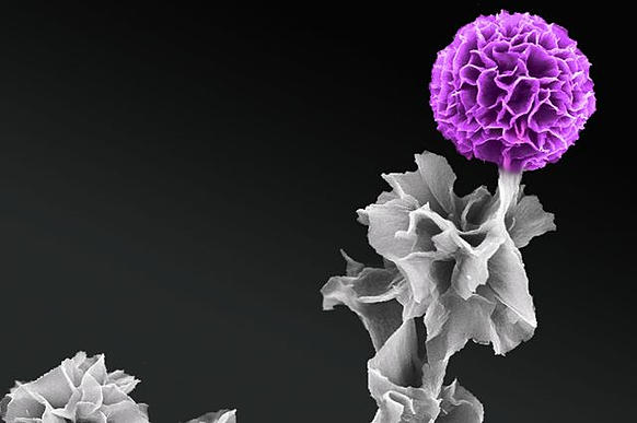
Their breakthrough was in creating an improved structure for one type of organic semiconductor, a building block of a conductive polymer called tetraaniline. The scientists showed for the first time that tetraaniline crystals could be grown vertically.

The advance could eventually lead to vastly improved technology for capturing solar energy. In fact, it could literally reshape solar cells. Scientists could potentially create “light antennas” — thin, pole-like devices that could absorb light from all directions, which would be an improvement over today’s wide, flat panels that can only absorb light from one surface.

The study, led by Richard Kaner, distinguished professor of chemistry and biochemistry and materials science and engineering, was recently published online by the journal ACS Nano.

The UCLA team grew the tetraaniline crystals vertically from a substrate, so the crystals stood up like spikes instead of lying flat as they do when produced using current techniques. They produced the crystals in a solution using a substrate made of graphene, a nanomaterial consisting of graphite that is extremely thin — measuring the thickness of a single atom. Scientists had previously grown crystals vertically in inorganic semiconducting materials, including silicon, but doing it in organic materials has been more difficult.

Tetraaniline is a desirable material for semiconductors because of its particular electrical and chemical properties, which are determined by the orientation of very small crystals it contains. Devices such as solar cells and photosensors work better if the crystals grow vertically because vertical crystals can be packed more densely in the semiconductor, making it more powerful and more efficient at controlling electrical current.

“These crystals are analogous to organizing a table covered with scattered pencils into a pencil cup,” said Yue “Jessica” Wang, a former UCLA doctoral student who now is a postdoctoral scholar at Stanford University and was the study’s first author. “The vertical orientation can save a great deal of space, and that can mean smaller, more efficient personal electronics in the near future.”
Once Kaner and his colleagues found they could guide the tetraaniline solution to grow vertical crystals, they developed a one-step method for growing highly ordered, vertically aligned crystals for a variety of organic semiconductors using the same graphene substrate.

“The key was deciphering the interactions between organic semiconductors and graphene in various solvent environments,” Wang said. “Once we understood this complex mechanism, growing vertical organic crystals became simple.”

Kaner said the researchers also discovered another advantage of the graphene substrate.
“This technique enables us to pattern crystals wherever we want,” he said. “You could make electronic devices from these semiconductor crystals and grow them precisely in intricate patterns required for the device you want, such as thin-film transistors or light-emitting diodes.”

The paper’s other authors were UCLA graduate students James Torres, Shan Jiang and Michael Yeung; Adam Stieg, associate director of shared resources at CNSI and the scientific director of the Nano and Pico Characterization Lab; Yves Rubin, UCLA professor of chemistry and biochemistry; and Xiangfeng Duan, UCLA professor of chemistry and biochemistry. Co-author Santanu Chaudhuri is a principal research scientist at the Illinois Applied Research Institute at University of Illinois at Urbana–Champaign.


Thursday, September 24, 2015

Designed defects in liquid crystals can guide construction of nanomaterials


Imperfections running through liquid crystals can be used as miniscule tubing, channeling molecules into specific positions to form new materials and nanoscale structures, according to engineers at the University of Wisconsin-Madison. The discovery could have applications in fields as diverse as electronics and medicine.
"By controlling the geometry of the system, we can send these channels from any one point to any other point," says Nicholas Abbott, a UW-Madison professor of chemical and biological engineering. "It's quite a versatile approach."
Photo: Nicholas Abbott
Nicholas Abbott
So far, Abbott and his collaborators at UW-Madison's Materials Research Science and Engineering Center (MRSEC) have been able to assemble phospholipids — molecules that can organize into layers in the walls of living cells — within liquid crystal defects.
Their technique may also be useful for assembling metallic wires and various semiconducting structures vital to electronics. There's also potential for mimicking the selective abilities of a membrane, designing a defect so that one type of molecule can pass through while others can't.
"This is an enabling discovery," Abbott says. "We're not looking for a specific application, but we're showing a versatile method of fabrication that can lead to structures you can't make any other way."
The researchers — including UW-Madison graduate students Xiaoguang Wang, Daniel S. Miller and Emre Bukusoglu, and Juan J. de Pablo, a former UW-Madison engineering professor now at the University of Chicago — published details of their advance this week in the journal Nature Materials.
For about 20 years, Abbott's research has examined the surfaces of soft materials, including liquid crystals — a particular phase of matter in which liquid-like materials also exhibit some of the molecular organization of solids.
"We've done a lot of work in the past at the interfaces of liquid crystals, but we're now looking inside the liquid crystal," he says. "We're looking at how to use the internal structure of liquid crystals to direct the organization of molecules. There's no prior example of using a defect in a liquid crystal to template molecular organization."
When the researchers manipulate the geometry of a liquid crystalline system, a variety of different defects can result. Abbott's group assembled liquid crystals with defects shaped like ropes or lines they call "disclinations," that formed templates they could fill with amphiphilic (water- and fat-loving) molecules.
Then they can link together assemblies of molecules and remove the liquid crystal templates, leaving behind the amphiphilic building blocks in a lasting, nanoscale structure.
The research is an example of how liquid crystal research is taking us from the nano to macro world, says Dan Finotello, program director at the National Science Foundation, which funds the MRSEC.
"It is also an exquisite demonstration of MRSEC programs' high impact," Finotello says. "MRSECs bring together several researchers of varied experience and complementary expertise who are then able to advance science at a considerably faster rate."

Monday, January 27, 2014

Swiss cheese crystal, or high-tech sponge?


Created by chemists at the University at Buffalo and Penn
State Hazleton, this sponge-like crystal contains many
pores that change shape when exposed to ultraviolet (UV) light.
Credit: Ian M. Walton

The remarkable properties of a new, porous material could lead to advances in microscopic sponging
The sponges of the future will do more than clean house.
Picture this, for example: Doctors use a tiny sponge to soak up a drug and deliver it directly to a tumor. Chemists at a manufacturing plant use another to trap and store unwanted gases.
These technologies are what University at Buffalo Assistant Professor of Chemistry Jason Benedict, PhD, had in mind when he led the design of a new material called UBMOF-1. The material — a metal-organic framework, or “MOF” — is a hole-filled crystal that could act as a sponge, capturing molecules of specific sizes and shapes in its pores.
Swiss cheese-like MOFs are not new, but Benedict’s has a couple of remarkable qualities:
  • The crystal’s pores change shape when hit by ultraviolet light. This is important because changing the pore structure is one way to control which compounds can enter or exit the pores. You could, for instance, soak up a chemical and then alter the pore size to prevent it from escaping. Secure storage is useful in applications like drug delivery, where “you don’t want the chemicals to come out until they get where they need to be,” Benedict says.
  • The crystal also changes color in response to ultraviolet light, going from colorless to red. This suggests that the material’s electronic properties are shifting, which could affect the types of chemical compounds that are attracted into the pores.
Benedict’s team reported on the creation of the UBMOF on Jan. 22 in the journal Chemical Communications. The paper’s coauthors include chemists from UB and Penn State Hazleton.
“MOFs are like molecular sponges — they’re crystals that have pores,” Benedict said.
“Typically, they are these passive materials: They’re static. You synthesize them, and that’s the end of the road,” he added. “What we’re trying to do is to take these passive materials and make them active, so that when you apply a stimulus like light, you can make them change their chemical properties, including the shape of their pores.”
Benedict is a member of UB’s New York State Center of Excellence in Materials Informatics, which the university launched in 2012 to advance the study of new materials that could improve life for future generations.
To force UBMOF-1 respond to ultraviolet light, Benedict and colleagues used some clever synthetic chemistry.
MOF crystals are made from two types of parts — metal nodes and organic rods — and the researchers attached a light-responsive chemical group called a diarylethene to the organic component of their material.
Diarylethene is special because it houses a ring of atoms that is normally open but shuts when exposed to ultraviolet light.
In the UBMOF, the diarylethene borders the crystal’s pores, which means the pores change shape when the diarylethene does.
The next step in the research is to determine how, exactly, the structure of the holes is changing, and to see if there’s a way to get the holes to revert to their original shape.
Rods containing diarylethene can be forced back into the “open” configuration with white light, but this tactic only works when the rods are alone. Once they’re inserted into the crystal, the diarylethene rings stay stubbornly closed in the presence of white light.
Source: http://www.buffalo.edu/news/releases/2014/01/031.html

Thursday, December 19, 2013

Liquid Crystal 'Flowers' That Can Be Used as Lenses

A team of material scientists, chemical engineers and physicists from the University of Pennsylvania has made another advance in their effort to use liquid crystals as a medium for assembling structures.
In their earlier studies, the team produced patterns of “defects,” useful disruptions in the repeating patterns found in liquid crystals, in nanoscale grids and rings. The new study adds a more complex pattern out of an even simpler template: a three-dimensional array in the shape of a flower.      
And because the petals of this “flower” are made of transparent liquid crystal and radiate out in a circle from a central point, the ensemble resembles a compound eye and can thus be used as a lens.  
The team consists of Randall Kamien, professor in the School of Arts and Sciences’ Department of Physics and Astronomy; Kathleen Stebe, the School of Engineering and Applied Science’s deputy dean for research and professor in Chemical and Biomolecular Engineering and Shu Yang, professor in Engineering’s departments of Materials Science and Engineering and Chemical and Biomolecular Engineering. Members of their labs also contributed to the new study, including lead author Daniel Beller, Mohamed Gharbi and Apiradee Honglawan.    
Their work was published in Physical Review X.   
The researchers’ ongoing work with liquid crystals is an example of a growing field of nanotechnology known as “directed assembly,” in which scientists and engineers aim to manufacture structures on the smallest scales without having to individually manipulate each component. Rather, they set out precisely defined starting conditions and let the physics and chemistry that govern those components do the rest.  
The starting conditions in the researchers previous experiments were templates consisting of tiny posts. In one of their studies, they showed that changing the size, shape or spacing of these posts would result in corresponding changes in the patterns of defects on the surface of the liquid crystal resting on top of them. In another experiment, they showed they could make a “hula hoop” of defects around individual posts, which would then act as a second template for a ring of defects at the surface.
In their latest work, the researchers used a much simpler cue.    
“Before we were growing these liquid crystals on something like a trellis, a template with precisely ordered features,” Kamien said. “Here, we’re just planting a seed.”
The seed, in this case, were silica beads — essentially, polished grains of sand. Planted at the top of a pool of liquid crystal flower-like patterns of defects grow around each bead.
The key difference between the template in this experiment and ones in the research team’s earlier work was the shape of the interface between the template and the liquid crystal.
In their experiment that generated grid patterns of defects, those patterns stemmed from cues generated by the templates’ microposts. Domains of elastic energy originated on the flat tops and edges of these posts and travelled up the liquid crystal’s layers, culminating in defects. Using a bead instead of a post, as the researchers did in their latest experiment, makes it so that the interface is no longer flat.             
“Not only is the interface at an angle, it’s an angle that keeps changing,” Kamien said. “The way the liquid crystal responds to that is that it makes these petal-like shapes at smaller and smaller sizes, trying to match the angle of the bead until everything is flat.”
Surface tension on the bead also makes it so these petals are arranged in a tiered, convex fashion. And because the liquid crystal can interact with light, the entire assembly can function as a lens, focusing light to a point underneath the bead.
“It’s like an insect’s compound eye, or the mirrors on the biggest telescopes,” said Kamien. “As we learn more about these systems, we’re going to be able to make these kinds of lenses to order and use them to direct light.”
This type of directed assembly could be useful in making optical switches and in other applications.
The research was supported by the National Science Foundation, Penn’s Materials Science Research and Engineering Center and the Simons Foundation.

Wednesday, October 9, 2013

Crystal Mysteries Spiral Deeper

New York University chemists have discovered crystal growth complexities, which at first glance appeared to confound 50 years of theory and deepened the mystery of how organic crystals form. But, appearances can be deceiving.
Their findings, which appear in the latest edition of Proceedings of the National Academy of Sciences, have a range of implications—from the production of pharmaceuticals and new electronic materials to unraveling the pathways for kidney stone formation.
The researchers focused on L-cystine crystals, the chief component of a particularly nefarious kind of kidney stone. The authors hoped to improve their understanding of how these crystals form and grow in order to design therapeutic agents that inhibit stone formation.
While the interest in L-cystine crystals is limited to the biomedical arena, understanding the details of crystal growth, especially the role of defects—or imperfections in crystals—is critical to the advancement of emerging technologies that aim to use organic crystalline materials.
Scientists in the Molecular Design Institute in the NYU Department of Chemistry have been examining defects in crystals called screw dislocations – features on the surface of a crystal that resemble a spiraled ham.
Dislocations were first posed by William Keith Burton, Nicolás Cabrera, and Sir Frederick Charles Frank in the late 1940s as essential for crystal growth. The so-called BCF theory posited that crystals with one screw dislocation would form hillocks that resembled a spiral staircase while those with two screw dislocations would merge and form a structure similar to a Mayan pyramid—a series of stacked “island” surfaces that are closed off from each other.
Using atomic force microscopy, the Molecular Design Institute team examined both kinds of screw dislocations in L-cystine crystals at nanoscale resolution. Their results showed exactly the opposite of what BCF theory predicted—crystals with one screw dislocation seemed to form stacked hexagonal “islands” while those with two proximal screw dislocations produced a six-sided spiral staircase.
A re-examination of these micrographs by Molecular Design Institute scientist Alexander Shtukenberg, in combination with computer simulations, served to refine the actual crystal growth sequence and found that, in fact, BCF theory still held. In other words, while the crystals’ physical appearance seemed at odds with the long-standing theory, they actually did grow in a manner predicted decades ago.
“These findings are remarkable in that they didn’t, at first glance, make any sense,” said NYU Chemistry Professor Michael Ward, one of the authors of the publication. “They appeared to contradict 60 years of thinking about crystal growth, but in fact revealed that crystal growth is at once elegant and complex, with hidden features that must be extracted if it is to be understood. More importantly, this example serves as a warning that first impressions are not always correct.”
The research was supported by the National Science Foundation (CHE-0845526, DMR-1105000, and DMR-1206337) and by the NSF Materials Research Science and Engineering Center (MRSEC) Program (DMR-0820341).

Flawed Diamonds: Gems for New Technology

Using ultra-fast laser pulses, a team of researchers led by UA assistant professor Vanessa Huxter has made the first detailed observation of how energy travels through diamonds containing nitrogen-vacancy centers – promising candidates for a variety of technological advances such as quantum computing.

A team of researchers led by University of Arizona assistant professor Vanessa Huxter has made the first detailed observation of how energy travels through diamonds that contain nitrogen-vacancy centers – defects in which two adjacent carbon atoms in the diamond's crystal structure are replaced by a single nitrogen atom and an empty gap.
 
These "flaws" result in unexpected and attractive properties that have put such diamonds in the spotlight as promising candidates for a variety of technological advances.
 
The findings, published online in Nature Physics, could help scientists better understand the properties of these diamonds, which have potential applications ranging from quantum computing to the imaging of individual atoms in molecules. 
 
Defect centers are locations in the otherwise repetitive lattice of carbon atoms where other elements have taken the spot of carbon atoms. Such defects create, for example, canary diamonds in which nitrogen atoms have replaced carbon atoms. In the case of a nitrogen vacancy, a nitrogen atom sits next to an empty slot where a carbon atom is missing. 
 
"Some of these defects have interesting optical and electronic properties," said Huxter, who recently joined the UA's Department of Chemistry and Biochemistry and led the research during a postdoctoral fellowship funded by the Natural Sciences and Engineering Research Council of Canada. Huxter did the research with co-authors Graham Fleming and Dmitry Budker at the U.S. Department of Energy's Lawrence Berkeley National Laboratory and the University of California, Berkeley.
 
Huxter said because the nitrogen-vacancy defects can be manipulated with optical methods such as lasers, they could be used for computing, data storage, sensing and even advanced imaging techniques capable of revealing the structure of molecules. 
 
"In order to use this system for these applications, we have to understand its fundamental properties," said Huxter, whose team is the first to study the ultrafast dynamics in these crystals in real time. "To use these systems for quantum computing, you want to have to some idea of what we call vibrational modes, because they determine the local environment and may possibly be used for information processing." 
 
To understand what that means, one has to picture the crystal structure of a diamond: a three-dimensional lattice of carbon atoms forming a highly ordered and repetitive structure. But the atoms are not glued into place. Rather, they vibrate back and forth as if connected by tiny springs. Wherever a nitrogen-vacancy defect interrupts the uniform carbon lattice, the vibrational properties change in ways that can be manipulated, for example by laser pulses. 
 
"We use laser light to see what is happening in the system," Huxter said. "When we hit these things with ultrafast pulses, it's like hitting them with a hammer. We put a lot of energy into the system, and watch as that energy flows through it."
 
The laser pulse knocks the electrons in the nitrogen-vacancy centers into a higher level of energy, which physicists call the excited state. Over time, the electrons fall back into their ground state, in a process called relaxation, while dissipating the energy into their surroundings. 
 
To watch how vibrations influence the ultrafast relaxation of the system, Huxter's team used ultrafast laser pulses, because the relaxation occurs on a time scale of a few nanoseconds – billionths of a second.
 
Exactly how that energy moves through the crystal and how it influences the vibrations around the nitrogen-vacancy centers is crucial to figuring out how to take advantage of its properties, but nobody had ever been able to observe this process before. 
 
"This is the first time we have been able to directly observe the vibrational spectrum of the system in real time," Huxter said. 
 
With her team, she employed two-dimensional electronic spectroscopy, basically a way of creating two-dimensional correlation "maps" that allow the researchers to watch the system as it relaxes to the ground state. 
 
"Think of it as ultra-high-speed photography to freeze the action on a scale of atoms and molecules," Huxter said. "We can watch the energy flow through the system in real time, and take snapshots along the way. We can see where the energy is going in and where it is coming out."
 
In the world of ultrafast spectroscopy, which is reminiscent of the first high-speed photography developed by Edward Muybridge in the early 20th century to freeze the action of galloping horses, "nanoseconds are like a million years," Huxter said, thanks to laser pulses lasting only femtoseconds. A femtosecond is one millionth of one billionth of a second. "In our experiments we were able to observe vibrations local to the defect with femtosecond time resolution. Being able to directly follow these vibrations led to some surprising new results including that these vibrations are quantum mechanically coherent for thousands of femtoseconds."
 
"The question we ask is, what happens when you start replacing the atoms in the crystal?" Huxter explained. "Will you get a change in the elastic properties? Each nitrogen-vacancy center is like a softer region you can poke at. They absorb the laser energy where there was previously no absorption and we see all these extra vibrational modes we don't see in the rest of the crystal."
 
"In our scenario, the diamond is like a clear window. We look straight through it and only see the defects. We tailor our laser pulse to the absorption of the defects."

Tuesday, September 3, 2013

Advancing Graphene for Post-Silicon Computer Logic

Team of UC Riverside researchers pioneer new approach for graphene logic circuits

A team of researchers from the University of California, Riverside’s Bourns College of Engineering have solved a problem that previously presented a serious hurdle for the use of graphene in electronic devices.
microscopic image of graphene
Scanning electron microscopy image of graphene device used in the study. The scale bar is one micrometer. The UCR logo next to it is implemented with etched graphene.
Graphene is a single-atom thick carbon crystal with unique properties beneficial for electronics including extremely high electron mobility and phonon thermal conductivity. However, graphene does not have an energy band gap, which is a specific property of semiconductor materials that separate electrons from holes and allows a transistor implemented with a given material to be completely switched off.
A transistor implemented with graphene will be very fast but will suffer from leakage currents and power dissipation while in the off state because of the absence of the energy band gap. Efforts to induce a band-gap in graphene via quantum confinement or surface functionalization have not resulted in a breakthrough. That left scientists wondering whether graphene applications in electronic circuits for information processing were feasible.
The UC Riverside team – Alexander Balandin andRoger Lake, both electrical engineering professors, Alexander Khitun, an adjunct professor of electrical engineering, and Guanxiong Liu and Sonia Ahsan, both of whom earned their Ph.Ds from UC Riverside while working on this research – has eliminated that doubt.
“Most researchers have tried to change graphene to make it more like conventional semiconductors for applications in logic circuits,” Balandin said. “This usually results in degradation of graphene properties. For example, attempts to induce an energy band gap commonly result in decreasing electron mobility while still not leading to sufficiently large band gap.”
Alexander Balandin
Alexander Balandin, a professor of Electrical Engineering
“We decided to take alternative approach,” Balandin said. “Instead of trying to change graphene, we changed the way the information is processed in the circuits.”
The UCR team demonstrated that the negative differential resistance experimentally observed in graphene field-effect transistors allows for construction of viable non-Boolean computational architectures with the gap-less graphene. The negative differential resistance – observed under certain biasing schemes – is an intrinsic property of graphene resulting from its symmetric band structure. The advanced version of the paper with UCR findings can be accessed at http://arxiv.org/abs/1308.2931.
Modern digital logic, which is used in computers and cell phones, is based on Boolean algebra implemented in semiconductor switch-based circuits. It uses zeroes and ones for encoding and processing the information. However, the Boolean logic is not the only way to process information. The UC Riverside team proposed to use specific current-voltage characteristics of graphene for constructing the non-Boolean logic architecture, which utilizes the principles of the non-linear networks.
headshot of Roger Lake
Roger Lake, a professor of electrical engineering
The graphene transistors for this study were built and tested by Liu at Balandin’s Nano-Device Laboratory at UC Riverside. The physical processes leading to unusual electrical characteristics were simulated using atomistic models by Ahsan, who was working under Lake. Khitun provided expertise on non-Boolean logic architectures.
The atomistic modeling conducted in Lake’s group shows that the negative differential resistance appears not only in microscopic-size graphene devices but also at the nanometer-scale, which would allow for fabrication of extremely small and low power circuits.
The proposed approach for graphene circuits presents a conceptual change in graphene research and indicates an alternative route for graphene’s applications in information processing according to the UC Riverside team.