Showing posts with label phonon. Show all posts

Friday, March 7, 2014

Crystals Ripple in Response to Light

Infrared light triggers wavelike motions of atoms in a crystal
of boron nitride. The waves, called surface phonon
polaritons, can be measured with the arm of an
atomic force microscope. Image by Siyuan Chen
Light can trigger coordinated, wavelike motions of atoms in atom-thin layers of crystal, scientists have shown. The waves, called phonon polaritons, are far shorter than light waves and can be "tuned" to particular frequencies and amplitudes by varying the number of layers of crystal, they report in the early online edition of Science March 7.
These properties - observed in this class of material for the first time - open the possibility of using polaritons to convey information in tight spaces, create images at far finer resolution than is possible with light, and manage the flow of heat in nanoscale devices.
"A wave on the surface of water is the closest analogy," said Dimitri Basov, professor of physics at the University of California, San Diego, who led the project. "You throw a stone and you launch concentric waves that move outward. This is similar. Atoms are moving. The triggering event is illumination with light."
The team used infrared light to launch phonon polaritons across a material called hexagonal boron nitride - crystals that form sheet-like layers held together by the weakest of chemical bonds.
Siyuan Dai, a graduate student in Basov's research group who was responsible for much of the experimental work and is the first author of the report, focused an infrared laser on the tip of an atomic-force microscope as it scanned across this material, registering motions in the crystalline lattice.
The measurements revealed interference patterns created as the traveling waves reached edges of the material and reflected back. The amplitude and frequency of the waves depended on the number of layers in the crystal. Both properties will prove useful in the design of nanodevices.
"You can bounce these waves off edges. You can bounce them off defects. You can play all sorts of cool tricks with them. And of course, you can design the wavelength and amplitude of these oscillations in a way that suits your purpose," Basov said.
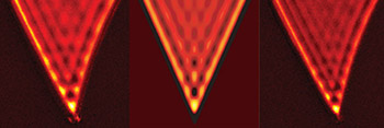
Interference patterns develop as surface phonon polaritons propagate across atom-thin layers of crystalline boron nitride and reflect back from edges.
The finding was something of a surprise. Boron nitride is an insulator used as a support structure for other materials, like graphene, which this group recently showed could support waves of electron densities called plasmon polaritons. Although similarly compact, plasmon polaritons rapidly dissipate.
"Because these materials are insulators, there is no electronic dissipation. So these waves travel further,” Basov said. “We didn’t expect them to be long-lived, but we are pleased that they are. It's becoming kind of practical."
Additional authors include Z. Fei, A.S. McLeod, M.K. Liu, M. Thiemens and M.M. Fogler of UC San Diego; Q. Ma and P. Jarillo-Herrero of MIT; A.S. Rodin of Boston University; W. Gannet, W. Regan and A. Zettl of UC Berkeley and Lawrence Berkeley National Laboratory; K. Watanabe and T. Taniguchi of the National Institute for Materials Science in Japan; Gerardo Dominguez of California State University, San Marcos; A.H. Castro Neto of Boston University and the National University of Singapore; and F. Keilmann of the Ludwig Maximilian University of Munich.
The U.S. Department of Energy, Office of Naval Research, Air Force Office of Scientific Research funded this work. Additional support for participating researchers came from NASA, NSF, and the National Research Programme. Keilmann is a co-founder of Neaspec, producer of the scanning nearfield optical microscope used in this study.
Source: http://ucsdnews.ucsd.edu/pressrelease/crystals_ripple_in_response_to_light

Tuesday, September 3, 2013

Advancing Graphene for Post-Silicon Computer Logic

Team of UC Riverside researchers pioneer new approach for graphene logic circuits

A team of researchers from the University of California, Riverside’s Bourns College of Engineering have solved a problem that previously presented a serious hurdle for the use of graphene in electronic devices.
microscopic image of graphene
Scanning electron microscopy image of graphene device used in the study. The scale bar is one micrometer. The UCR logo next to it is implemented with etched graphene.
Graphene is a single-atom thick carbon crystal with unique properties beneficial for electronics including extremely high electron mobility and phonon thermal conductivity. However, graphene does not have an energy band gap, which is a specific property of semiconductor materials that separate electrons from holes and allows a transistor implemented with a given material to be completely switched off.
A transistor implemented with graphene will be very fast but will suffer from leakage currents and power dissipation while in the off state because of the absence of the energy band gap. Efforts to induce a band-gap in graphene via quantum confinement or surface functionalization have not resulted in a breakthrough. That left scientists wondering whether graphene applications in electronic circuits for information processing were feasible.
The UC Riverside team – Alexander Balandin andRoger Lake, both electrical engineering professors, Alexander Khitun, an adjunct professor of electrical engineering, and Guanxiong Liu and Sonia Ahsan, both of whom earned their Ph.Ds from UC Riverside while working on this research – has eliminated that doubt.
“Most researchers have tried to change graphene to make it more like conventional semiconductors for applications in logic circuits,” Balandin said. “This usually results in degradation of graphene properties. For example, attempts to induce an energy band gap commonly result in decreasing electron mobility while still not leading to sufficiently large band gap.”
Alexander Balandin
Alexander Balandin, a professor of Electrical Engineering
“We decided to take alternative approach,” Balandin said. “Instead of trying to change graphene, we changed the way the information is processed in the circuits.”
The UCR team demonstrated that the negative differential resistance experimentally observed in graphene field-effect transistors allows for construction of viable non-Boolean computational architectures with the gap-less graphene. The negative differential resistance – observed under certain biasing schemes – is an intrinsic property of graphene resulting from its symmetric band structure. The advanced version of the paper with UCR findings can be accessed at http://arxiv.org/abs/1308.2931.
Modern digital logic, which is used in computers and cell phones, is based on Boolean algebra implemented in semiconductor switch-based circuits. It uses zeroes and ones for encoding and processing the information. However, the Boolean logic is not the only way to process information. The UC Riverside team proposed to use specific current-voltage characteristics of graphene for constructing the non-Boolean logic architecture, which utilizes the principles of the non-linear networks.
headshot of Roger Lake
Roger Lake, a professor of electrical engineering
The graphene transistors for this study were built and tested by Liu at Balandin’s Nano-Device Laboratory at UC Riverside. The physical processes leading to unusual electrical characteristics were simulated using atomistic models by Ahsan, who was working under Lake. Khitun provided expertise on non-Boolean logic architectures.
The atomistic modeling conducted in Lake’s group shows that the negative differential resistance appears not only in microscopic-size graphene devices but also at the nanometer-scale, which would allow for fabrication of extremely small and low power circuits.
The proposed approach for graphene circuits presents a conceptual change in graphene research and indicates an alternative route for graphene’s applications in information processing according to the UC Riverside team.