Showing posts with label Microchips. Show all posts

Monday, June 20, 2016

Particle accelerator on a microchip

Three “accelerators on a chip” made of silicon are mounted on a clear base. Credit: SLAC National Accelerator Laboratory

The Gordon and Betty Moore Foundation has awarded 13.5 million US dollars (12.6 million euros) to promote the development of a particle accelerator on a microchip. DESY and the University of Hamburg are among the partners involved in this international project, headed by Robert Byer of Stanford University (USA) and Peter Hommelhoff of the University of Erlangen-Nürnberg. Within five years, they hope to produce a working prototype of an “accelerator-on-a-chip”.

For decades, particle accelerators have been an indispensable tool in countless areas of research – from fundamental research in physics to examining the structure of biomolecules in order to develop new drugs. Accelerator-based research has repeatedly been awarded Nobel prizes. Until now, the necessary facilities have been very large and costly. Scientists and engineers are trying out a range of different approaches to build more compact and less expensive particle accelerators. For the time being, the big facilities will remain indispensable for many purposes, however there are some applications in which efficient miniature electron accelerators can provide completely new insights.

“The impact of shrinking accelerators can be compared to the evolution of computers that once occupied entire rooms and can now be worn around your wrist,” says Hommelhoff. This advance could mean that particle accelerators will become available in areas that have previously had no access to such technologies.

The aim of the project is to develop a new type of small, inexpensive particle accelerator for a wide range of different users. Apart from using the fast electrons themselves, they could also be used to produce high-intensity X-rays. “This prototype could set the stage for a new generation of ‘tabletop’ accelerators, with unanticipated discoveries in biology and materials science and potential applications in security scanning, medical therapy and X-ray imaging,” explains Byer.

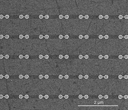
Some of the accelerator-on-a-chip designs being explored by the international collaboration. Credit: SLAC National Accelerator Laboratory


The project is based on advances in nano-photonics, the art of creating and using nano structures to generate and manipulate different kinds of light. A laser using visible or infrared light is used to accelerate the electrically charged elementary particles, rather than the radio-frequency (RF) waves currently used. The wavelength of this radiation is some ten to one hundred thousand times shorter than that of the radio waves, meaning that steeper accelerator gradients can be achieved than those using RF technology. “The advantage is that everything is up to fifty times smaller,” explains Franz Kärtner who is a Leading Scientist at DESY, as well as a professor at the University of Hamburg and the Massachusetts Institute of Technology (MIT) in the US, and a member of Hamburg’s Centre for Ultrafast Imaging (CUI), and who heads a similar project in Hamburg, funded by the European Research Council.

“The typical transverse dimensions of an accelerator cell shrink from ten centimetres to one micrometre,” adds Ingmar Hartl, head of the laser group in DESY’s Photon Science Division. At the moment, the material of choice for the miniature accelerator modules is silicon. “The advantage is that we can draw on the highly advanced production technologies that are already available for silicon microchips,” explains Hartl.

DESY will bring its vast knowhow as an internationally leader in laser technology to the project, which has already paid off in other collaborations involving the University of Erlangen-Nürnberg. There, Hommelhoff’s group showed that for slow electrons a micro-structured accelerator module is able to achieve steeper acceleration gradients than RF technology.

Byer’s group had demonstrated independently the same effect for fast, so-called relativistic electrons.

However, it is still a long way from an experimental set-up in a laboratory to a working prototype. Individual components of the system will have to be developed from scratch.

Among other things, DESY is working on a high-precision electron source to feed the elementary particles into the accelerator modules, a powerful laser for accelerating them, and an electron undulator for creating X-rays. In addition, the interaction between the miniature components is not yet a routine matter, especially not when it comes to joining up several accelerator modules.

The SINBAD (“Short Innovative Bunches and Accelerators at DESY”) accelerator lab that is currently being set up at DESY will provide the ideal testing environment for the miniature accelerator modules. “SINBAD will allow us to feed high-quality electron beams into the modules, to test the quality of the radiation and work out an efficient way of coupling the laser.

DESY offers unique opportunities in this respect,” explains Ralph Aßmann, Leading Scientist at DESY.

Apart from DESY, the Universities of Stanford, Erlangen-Nürnberg and Hamburg, SLAC National Accelerator Laboratory in the US, the Swiss Paul Scherrer Institute (PSI) and the University of California in Los Angeles (UCLA), the Purdue University, the Swiss Federal Institute of Technology in Lausanne (EPFL) and the Technical University of Darmstadt are also involved in the project, as well as the US company Tech-X.

The Gordon and Betty Moore Foundation fosters path-breaking scientific discovery, environmental conservation, patient care improvements and the preservation of the special character of the San Francisco Bay Area. Gordon Moore is one of the founders of the chip manufacturer Intel and the author of “Moore's Law”, which predicts that the number of transistors in an integrated circuit doubles approximately every two years.

DESY

Read on NTWA

Wednesday, June 10, 2015

Rice researchers make ultrasensitive conductivity measurements


Researchers at Rice University have discovered a new way to make ultrasensitive conductivity measurements at optical frequencies on high-speed nanoscale electronic components.

The research at Rice’s Laboratory for Nanophotonics (LANP) is described online in a new study in the American Chemical Society’s journal ACS Nano. In a series of experiments, LANP researchers linked pairs of puck-shaped metal nanodisks with metallic nanowires and showed how the flow of current at optical frequencies through the nanowires produced “charge transfer plasmons” with unique optical signatures.

“The push to continually increase the speed of microchip components has researchers looking at nanoscale devices and components that operate at optical frequencies for next-generation electronics,” said LANP Director Naomi Halas, the lead scientist on the study. “It is not well-known how these materials and components operate at extremely high frequencies of light, and LANP’s new technique provides a way to measure the electrical transport properties of nanomaterials and structures at these extremely high frequencies.”

Read more: http://www.nanotechnologyworld.org/#!Rice-researchers-make-ultrasensitive-conductivity-measurements/c89r/5578553e0cf2df2eae412b28 

Wednesday, January 22, 2014

Cooling Microprocessors with Carbon Nanotubes

“Cool it!” That’s a prime directive for microprocessor chips and a promising new solution to meeting this imperative is in the offing. Researchers with the U.S. Department of Energy (DOE)’s Lawrence Berkeley National Laboratory (Berkeley Lab) have developed a “process friendly” technique that would enable the cooling of microprocessor chips through carbon nanotubes.

Frank Ogletree, a physicist with Berkeley Lab’s Materials Sciences Division, led a study in which organic molecules were used to form strong covalent bonds between carbon nanotubes and metal surfaces. This improved by six-fold the flow of heat from the metal to the carbon nanotubes, paving the way for faster, more efficient cooling of computer chips. The technique is done through gas vapor or liquid chemistry at low temperatures, making it suitable for the manufacturing of computer chips.

“We’ve developed covalent bond pathways that work for oxide-forming metals, such as aluminum and silicon, and for more noble metals, such as gold and copper,” says Ogletree, who serves as a staff engineer for the Imaging Facility at the Molecular Foundry, a DOE nanoscience center hosted by Berkeley Lab. “In both cases the mechanical adhesion improved so that surface bonds were strong enough to pull a carbon nanotube array off of its growth substrate and significantly improve the transport of heat across the interface.”
Ogletree is the corresponding author of a paper describing this research in Nature Communications. The paper is titled “Enhanced Thermal Transport at Covalently Functionalized Carbon Nanotube Array Interfaces.” Co-authors are Sumanjeet Kaur, Nachiket Raravikar, Brett Helms and Ravi Prasher.

Overheating is the bane of microprocessors. As transistors heat up, their performance can deteriorate to the point where they no longer function as transistors. With microprocessor chips becoming more densely packed and processing speeds continuing to increase, the overheating problem looms ever larger. The first challenge is to conduct heat out of the chip and onto the circuit board where fans and other techniques can be used for cooling. Carbon nanotubes have demonstrated exceptionally high thermal conductivity but their use for cooling microprocessor chips and other devices has been hampered by high thermal interface resistances in nanostructured systems.

From left, Brett Helms, Frank Ogletree and Sumanjeet Kaur at the Molecular Foundry used organic molecules to form strong covalent bonds between carbon nanotubes and metal surfaces, improving by six-fold the flow of heat from the metal to the carbon nanotubes. (Photo by Roy Kaltschmidt)
“The thermal conductivity of carbon nanotubes exceeds that of diamond or any other natural material but because carbon nanotubes are so chemically stable, their chemical interactions with most other materials are relatively weak, which makes for  high thermal interface resistance,” Ogletree says. “Intel came to the Molecular Foundry wanting to improve the performance of carbon nanotubes in devices. Working with Nachiket Raravikar and Ravi Prasher, who were both Intel engineers when the project was initiated, we were able to increase and strengthen the contact between carbon nanotubes and the surfaces of other materials. This reduces thermal resistance and substantially improves heat transport efficiency.”

Sumanjeet Kaur, lead author of the Nature Communications paper and an expert on carbon nanotubes, with assistance from co-author and Molecular Foundry chemist Brett Helms, used reactive molecules to bridge the carbon nanotube/metal interface – aminopropyl-trialkoxy-silane (APS) for oxide-forming metals, and cysteamine for noble metals. First vertically aligned carbon nanotube arrays were grown on silicon wafers, and thin films of aluminum or gold were evaporated on glass microscope cover slips. The metal films were then “functionalized” and allowed to bond with the carbon nanotube arrays. Enhanced heat flow was confirmed using a characterization technique developed by Ogletree that allows for interface-specific measurements of heat transport.

“You can think of interface resistance in steady-state heat flow as being an extra amount of distance the heat has to flow through the material,” Kaur says. “With carbon nanotubes, thermal interface resistance adds something like 40 microns of distance on each side of the actual carbon nanotube layer. With our technique, we’re able to decrease the interface resistance so that the extra distance is around seven microns at each interface.”

Although the approach used by Ogletree, Kaur and their colleagues substantially strengthened the contact between a metal and individual carbon nanotubes within an array, a majority of the nanotubes within the array may still fail to connect with the metal. The Berkeley team is now developing a way to improve the density of carbon nanotube/metal contacts. Their technique should also be applicable to single and multi-layer graphene devices, which face the same cooling issues.

“Part of our mission at the Molecular Foundry is to help develop solutions for technology problems posed to us by industrial users that also raise fundamental science questions,” Ogletree says. “In developing this technique to address a real-world technology problem, we also created tools that yield new information on fundamental chemistry.”
This work was supported by the DOE Office of Science and the Intel Corporation.
#  #  #
The Molecular Foundry is one of five DOE Nanoscale Science Research Centers (NSRCs), national user facilities for interdisciplinary research at the nanoscale, supported by the DOE Office of Science. Together the NSRCs comprise a suite of complementary facilities that provide researchers with state-of-the-art capabilities to fabricate, process, characterize, and model nanoscale materials, and constitute the largest infrastructure investment of the National Nanotechnology Initiative. The NSRCs are located at DOE’s Argonne, Brookhaven, Lawrence Berkeley, Oak Ridge and Sandia and Los Alamos national laboratories. 

Lawrence Berkeley National Laboratory addresses the world’s most urgent scientific challenges by advancing sustainable energy, protecting human health, creating new materials, and revealing the origin and fate of the universe. Founded in 1931, Berkeley Lab’s scientific expertise has been recognized with 13 Nobel prizes. The University of California manages Berkeley Lab for the U.S. Department of Energy’s Office of Science. For more, visit www.lbl.gov.

The DOE Office of Science is the single largest supporter of basic research in the physical sciences in the United States and is working to address some of the most pressing challenges of our time. For more information, please visit science.energy.gov.

Source: http://newscenter.lbl.gov/news-releases/2014/01/22/cooling-microprocessors-with-carbon-nanotubes/

Monday, August 26, 2013

Cost-saving computer chips get smaller than ever

Not so long ago, a computer filled a whole room and radio receivers were as big as washing machines. In recent decades, electronic devices have shrunk considerably in size and this trend is expected to continue, leading to enormous cost and energy savings, as well as increasing speed. 

Key to shrinking devices is Terascale computing, involving ultrafast technology supported by single microchips that can perform trillions of operations per second. 

Using Terascale technology, semiconductor components commonly used to make integrated circuits for all kinds of appliances could measure less than 10 nanometers within several years. Keeping in mind that a nanometer is less than 1 billionth of a meter, electronic devices have the potential to become phenomenally smaller and require significantly less energy than today - a development that will revolutionise the electronics industry. 

Despite progress, the technology for producing these ultra-small devices has a long way to go before being reliable. To advance the work, the EU-funded project TRAMS ('Terascale reliable adaptive memory systems') sought to improve reliability by improving chip design. 

The TRAMS team conducted in-depth variability and reliability analyses to develop chip circuits that are much less prone to errors. These circuits feature new designs that yield reliable memory systems from currently unreliable nanodevices. 

The main challenge was to develop reliable, energy efficient and cost effective computing using a variety of new technologies with individual transistors potentially measuring below five nanometers in size. 

The team investigated a number of technologies and materials with potential to make Terascale computing a reality. These included: 

- carbon nanotubes (very tiny cylindrical nanostructures grapheme technology); 
- new transistor geometries, such as FinFETs; 
- state-of-the-art nanowires, which offer very advanced transistor capabilities for use in a new generation of electronic devices. 

Using models, the researchers analysed reliability - from the technology to the circuit level. 

These advances are expected to redefine today's standard 'complementary metal-oxide semiconductors' (CMOS). The team's results would help Europe's manufacturers develop CMOS devices below the 16 nanometre range. The biggest challenge will lie in reducing CMOS devices to below five nanometres - a development that now starts to look possible. 

From communication and security to transport and industry, CMOS-based devices of the future promise to redesign the technology we use, introducing radical energy and cost savings. 

The TRAMS consortium includes universities and companies from Spain, Belgium and the UK. The project was coordinated by Spain's Universitat Politècnica de Catalunya, and received almost EUR 2.5 million in EU funding. The team concluded its work in December 2012.

http://trams-project.upc.edu/