Showing posts with label cleantech. Show all posts

Monday, December 7, 2015

Nanostructured germanium for portable photovoltaics and battery electrodes


New approaches for hybrid solar cells


Using a new procedure researchers at the Technical University of Munich (TUM) and the Ludwig Maximillians University of Munich (LMU) can now produce extremely thin and robust, yet highly porous semiconductor layers. A very promising material – for small, light-weight, flexible solar cells, for example, or electrodes improving the performance of rechargeable batteries.

The coating on the wafer that Professor Thomas Fässler, chair of Inorganic Chemistry with a Focus on Novel Materials at TU Munich, holds in his hands glitters like an opal. And it has amazing properties: It is hard as a crystal, exceptionally thin and – since it is highly porous – light as a feather.

By integrating suitable organic polymers into the pores of the material, the scientists can custom tailor the electrical properties of the ensuing hybrid material. The design not only saves space, it also creates large interface surfaces that improve overall effectiveness.

“You can imagine our raw material as a porous scaffold with a structure akin to a honeycomb. The walls comprise inorganic, semiconducting germanium, which can produce and store electric charges. Since the honeycomb walls are extremely thin, charges can flow along short paths,” explains Fässler.

The new design: bottom-up instead of top-down

But, to transform brittle, hard germanium into a flexible and porous layer the researchers had to apply a few tricks. Traditionally, etching processes are used to structure the surface of germanium. However, this top-down approach is difficult to control on an atomic level. The new procedure solves this problem.

Together with his team, Fässler established a synthesis methodology to fabricate the desired structures very precisely and reproducibly. The raw material is germanium with atoms arranged in clusters of nine. Since these clusters are electrically charged, they repel each other as long as they are dissolved. Netting only takes place when the solvent is evaporated.

This can be easily achieved by applying heat of 500 °C or it can be chemically induced, by adding germanium chloride, for example. By using other chlorides like phosphorous chloride the germanium structures can be easily doped. This allows the researchers to directly adjust the properties of the resulting nanomaterials in a very targeted manner.

Tiny synthetic beads as nanotemplates

To give the germanium clusters the desired porous structure, the LMU researcher Dr. Dina Fattakhova-Rohlfing has developed a methodology to enable nanostructuring: Tiny polymer beads form three-dimensional templates in an initial step.

In the next step, the germanium-cluster solution fills the gaps between the beads. As soon as stable germanium networks have formed on the surface of the tiny beads, the templates are removed by applying heat. What remains is the highly porous nanofilm.

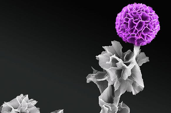
The deployed polymer beads have a diameter of 50 to 200 nanometers and form an opal structure. The germanium scaffold that emerges on the surface acts as a negative mold – an inverse opal structure is formed. Thus, the nanolayers glitter like an opal.

“The porous germanium alone has unique optical and electrical properties that many energy relevant applications can profit from,” says LMU researcher Dr. Dina Fattakhova-Rohlfing, who, in collaboration with Fässler, developed the material. “Beyond that, we can fill the pores with a wide variety of functional materials, thereby creating a broad range of novel hybrid materials.”


Nanolayers pave the road to portable photovoltaic solutions

“When combined with polymers, porous germanium structures are suitable for the development of a new generation of stable, extremely light-weight and flexible solar cells that can charge mobile phones, cameras and laptops while on the road,” explains the physicist Peter Müller-Buschbaum, professor of functional materials at TU Munich.

Manufacturers around the world are on the lookout for light-weight and robust materials to use in portable solar cells. To date they have used primarily organic compounds, which are sensitive and have relatively short lifetimes. Heat and light decompose the polymers and cause the performance to degrade. Here, the thin but robust germanium hybrid layers provide a real alternative.

Nanolayers for new battery systems

Next, the researchers want to use the new technology to manufacture highly porous silicon layers. The layers are currently being tested as anodes for rechargeable batteries. They could conceivably replace the graphite layers currently used in batteries to improve their capacity.

The research was funded by the “Solar Technologies Go Hybrid” program of the Bavarian State Ministry of Science, in the context of the excellence cluster “Nanosystems Initiative Munich (NIM), the German Research Foundation (DFG) and the Center for Nanosciences (CeNS).


Publication:

Zintl Clusters as Wet Chemical Precursors for Germanium Nanomorphologies with Tunable Composition; Manuel M. Bentlohner, Markus Waibel, Patrick Zeller, Kuhu Sarkar, Peter Müller-Buschbaum, Dina Fattakhova-Rohlfing, Thomas F. Fässler
Angewandte Chemie, online 03.12.2015 – DOI: 10.1002/ange.201508246


http://www.nanotechnologyworld.org/?draft=true#!Nanostructured-germanium-for-portable-photovoltaics-and-battery-electrodes/c89r/56659a740cf28314431b0321 

Friday, December 4, 2015

Storing electricity in paper


One sheet, 15 centimetres in diameter and a few tenths of a millimetre thick can store as much as 1 F, which is similar to the supercapacitors currently on the market. The material can be recharged hundreds of times and each charge only takes a few seconds.

It’s a dream product in a world where the increased use of renewable energy requires new methods for energy storage – from summer to winter, from a windy day to a calm one, from a sunny day to one with heavy cloud cover.

”Thin films that function as capacitors have existed for some time. What we have done is to produce the material in three dimensions. We can produce thick sheets,” says Xavier Crispin, professor of organic electronics and co-author to the article just published in Advanced Science.
Other co-authors are researchers from KTH Royal Institute of Technology, Innventia, Technical University of Denmark and the University of Kentucky.

The material, power paper, looks and feels like a slightly plasticky paper and the researchers have amused themselves by using one piece to make an origami swan – which gives an indication of its strength.

The structural foundation of the material is nanocellulose, which is cellulose fibres which, using high-pressure water, are broken down into fibres as thin as 20 nm in diameter. With the cellulose fibres in a solution of water, an electrically charged polymer (PEDOT:PSS), also in a water solution, is added. The polymer then forms a thin coating around the fibres.

”The covered fibres are in tangles, where the liquid in the spaces between them functions as an electrolyte,” explains Jesper Edberg, doctoral student, who conducted the experiments together with Abdellah Malti, who recently completed his doctorate.

The new cellulose-polymer material has set a new world record in simultaneous conductivity for ions and electrons, which explains its exceptional capacity for energy storage. It also opens the door to continued development toward even higher capacity. Unlike the batteries and capacitors currently on the market, power paper is produced from simple materials – renewable cellulose and an easily available polymer. It is light in weight, it requires no dangerous chemicals or heavy metals and it is waterproof.

The Power Papers project has been financed by the Knut and Alice Wallenberg Foundation since 2012.

”They leave us to our research, without demanding lengthy reports, and they trust us. We have a lot of pressure on us to deliver, but it’s ok if it takes time, and we’re grateful for that,” says Professor Magnus Berggren, director of the Laboratory of Organic Electronics at Linköping University.

The new power paper is just like regular pulp, which has to be dehydrated when making paper. The challenge is to develop an industrial-scale process for this.

”Together with KTH, Acreo and Innventia we just received SEK 34 million from the Swedish Foundation for Strategic Research to continue our efforts to develop a rational production method, a paper machine for power paper,” says Professor Berggren.

Power paper – Four world records

Highest charge and capacitance in organic electronics, 1 C and 2 F (Coulomb and Farad).
Highest measured current in an organic conductor, 1 A (Ampere).
Highest capacity to simultaneously conduct ions and electrons.
Highest transconductance in a transistor, 1 S (Siemens)

Publication:

An Organic Mixed Ion-Electron Conductor for Power Electronics, Abdellah Malti, Jesper Edberg, Hjalmar Granberg, Zia Ullah Khan, Jens W Andreasen, Xianjie Liu, Dan Zhao, Hao Zhang, Yulong Yao, Joseph W Brill, Isak Engquist, Mats Fahlman, Lars Wågberg, Xavier Crispin and Magnus Berggren.  Advanced Science, DOI 10.1002/advs.201500305

Thursday, October 15, 2015

Researchers Take First Steps to Create Biodegradable Displays for Electronics


Americans, on average, replace their mobile phones every 22 months, junking more than 150 million phones a year in the process. When it comes to recycling and processing all of this electronic waste, the World Health Organization reports that even low exposure to the electronic elements can cause significant health risks. Now,University of Missouri researchers are on the path to creating biodegradable electronics by using organic components in screen displays. The researchers’ advancements could one day help reduce electronic waste in the world’s landfills.

“Current mobile phones and electronics are not biodegradable and create significant waste when they’re disposed,” said Suchismita Guha, professor in the Department of Physics and Astronomy at the MU College of Arts and Science. “This discovery creates the first biodegradable active layer in organic electronics, meaning—in principle—we can eventually achieve full biodegradability.”

Guha, along with graduate student Soma Khanra, collaborated with a team from the Federal University of ABC (UFABC) in Brazil to develop organic structures that could be used to light handheld device screens. Using peptides, or proteins, researchers were able to demonstrate that these tiny structures, when combined with a blue light-emitting polymer, could successfully be used in displays.

“These peptides can self-assemble into beautiful nanostructures or nanotubes, and, for us, the main goal has been to use these nanotubes as templates for other materials,” Guha said. “By combining organic semiconductors with nanomaterials, we were able to create the blue light needed for a display. However, in order to make a workable screen for your mobile phone or other displays, we’ll need to show similar success with red and green light-emitting polymers.”

The scientists also discovered that by using peptide nanostructures they were able to use less of the polymer. Using less to create the same blue light means that the nanocomposites achieve almost 85 percent biodegradability.

“By using peptide nanostructures, which are 100 percent biodegradable, to create the template for the active layer for the polymers, we are able to understand how electronics themselves can be more biodegradable,” Guha said. “This research is the first step and the first demonstration of using such biology to improve electronics.”

The study “Self-Assembled Peptide-Polyfluorene Nanocomposites for Biodegradable Organic Electronics” recently was published as the inside cover article in Advanced Materials Interfaces.

The work was supported by the National Science Foundation (Grant IIA-1339011) and CNPq (400239/2014-0). The content is solely the responsibility of the authors and does not necessarily represent the official views of the funding agencies.

Tommi White, assistant research professor of biochemistry, and Thomas Lam, both with the Microscopy Core Research Facility at MU, contributed to the study. Other collaborators include Wendel A. Alves and Thiago Cipriano, professors of supramolecular chemistry at UFABC; Eudes E. Fileti, a professor of physics at the Federal University of São Paulo, Brazil.

University of Missouri

Quantum physics meets genetic engineering


Nature has had billions of years to perfect photosynthesis, which directly or indirectly supports virtually all life on Earth. In that time, the process has achieved almost 100 percent efficiency in transporting the energy of sunlight from receptors to reaction centers where it can be harnessed — a performance vastly better than even the best solar cells.

One way plants achieve this efficiency is by making use of the exotic effects of quantum mechanics — effects sometimes known as “quantum weirdness.” These effects, which include the ability of a particle to exist in more than one place at a time, have now been used by engineers at MIT to achieve a significant efficiency boost in a light-harvesting system.

Surprisingly, the MIT researchers achieved this new approach to solar energy not with high-tech materials or microchips — but by using genetically engineered viruses.

This achievement in coupling quantum research and genetic manipulation, described this week in the journal Nature Materials, was the work of MIT professors Angela Belcher, an expert on engineering viruses to carry out energy-related tasks, and Seth Lloyd, an expert on quantum theory and its potential applications; research associate Heechul Park; and 14 collaborators at MIT and in Italy.

Lloyd, a professor of mechanical engineering, explains that in photosynthesis, a photon hits a receptor called a chromophore, which in turn produces an exciton — a quantum particle of energy. This exciton jumps from one chromophore to another until it reaches a reaction center, where that energy is harnessed to build the molecules that support life.

But the hopping pathway is random and inefficient unless it takes advantage of quantum effects that allow it, in effect, to take multiple pathways at once and select the best ones, behaving more like a wave than a particle.


This efficient movement of excitons has one key requirement: The chromophores have to be arranged just right, with exactly the right amount of space between them. This, Lloyd explains, is known as the “Quantum Goldilocks Effect.”

That’s where the virus comes in. By engineering a virus that Belcher has worked with for years, the team was able to get it to bond with multiple synthetic chromophores — or, in this case, organic dyes. The researchers were then able to produce many varieties of the virus, with slightly different spacings between those synthetic chromophores, and select the ones that performed best.

In the end, they were able to more than double excitons’ speed, increasing the distance they traveled before dissipating — a significant improvement in the efficiency of the process.

The project started from a chance meeting at a conference in Italy. Lloyd and Belcher, a professor of biological engineering, were reporting on different projects they had worked on, and began discussing the possibility of a project encompassing their very different expertise. Lloyd, whose work is mostly theoretical, pointed out that the viruses Belcher works with have the right length scales to potentially support quantum effects.

In 2008, Lloyd had published a paper demonstrating that photosynthetic organisms transmit light energy efficiently because of these quantum effects. When he saw Belcher’s report on her work with engineered viruses, he wondered if that might provide a way to artificially induce a similar effect, in an effort to approach nature’s efficiency.

“I had been talking about potential systems you could use to demonstrate this effect, and Angela said, ‘We’re already making those,’” Lloyd recalls. Eventually, after much analysis, “We came up with design principles to redesign how the virus is capturing light, and get it to this quantum regime.”

Within two weeks, Belcher’s team had created their first test version of the engineered virus. Many months of work then went into perfecting the receptors and the spacings.

Once the team engineered the viruses, they were able to use laser spectroscopy and dynamical modeling to watch the light-harvesting process in action, and to demonstrate that the new viruses were indeed making use of quantum coherence to enhance the transport of excitons.

“It was really fun,” Belcher says. “A group of us who spoke different [scientific] languages worked closely together, to both make this class of organisms, and analyze the data. That’s why I’m so excited by this.”

While this initial result is essentially a proof of concept rather than a practical system, it points the way toward an approach that could lead to inexpensive and efficient solar cells or light-driven catalysis, the team says. So far, the engineered viruses collect and transport energy from incoming light, but do not yet harness it to produce power (as in solar cells) or molecules (as in photosynthesis). But this could be done by adding a reaction center, where such processing takes place, to the end of the virus where the excitons end up.

“This is exciting and high-quality research,” says Alán Aspuru-Guzik, a professor of chemistry and chemical biology at Harvard University who was not involved in this work. The research, he says, “combines the work of a leader in theory (Lloyd) and a leader in experiment (Belcher) in a truly multidisciplinary and exciting combination that spans biology to physics to potentially, future technology.”

“​Access to controllable excitonic systems is a goal shared by many researchers in the field,” Aspuru-Guzik adds. “This work provides fundamental understanding that can allow for the development of devices with an increased control of exciton flow.”

The research was supported by the Italian energy company Eni through the MIT Energy Initiative. In addition to MIT postdocs Nimrod Heldman and Patrick Rebentrost, the team included researchers at the University of Florence, the University of Perugia, and Eni.

Friday, October 2, 2015

Scientists grow organic semiconductor crystals vertically for first time


UCLA-led breakthrough could literally reshape solar cells and electronic devices


Our smartphones, tablets, computers and biosensors all have improved because of the rapidly increasing efficiency of semiconductors.

Since the turn of the 21st century, organic, or carbon-based, semiconductors have emerged as a major area of interest for scientists because they are inexpensive, plentiful and lightweight, and they can conduct current in ways comparable to inorganic semiconductors, which are made from metal-oxides or silicon.

Now, materials scientists from the California NanoSystems Institute at UCLA have discovered a way to make organic semiconductors more powerful and more efficient.

Their breakthrough was in creating an improved structure for one type of organic semiconductor, a building block of a conductive polymer called tetraaniline. The scientists showed for the first time that tetraaniline crystals could be grown vertically.

The advance could eventually lead to vastly improved technology for capturing solar energy. In fact, it could literally reshape solar cells. Scientists could potentially create “light antennas” — thin, pole-like devices that could absorb light from all directions, which would be an improvement over today’s wide, flat panels that can only absorb light from one surface.

The study, led by Richard Kaner, distinguished professor of chemistry and biochemistry and materials science and engineering, was recently published online by the journal ACS Nano.

The UCLA team grew the tetraaniline crystals vertically from a substrate, so the crystals stood up like spikes instead of lying flat as they do when produced using current techniques. They produced the crystals in a solution using a substrate made of graphene, a nanomaterial consisting of graphite that is extremely thin — measuring the thickness of a single atom. Scientists had previously grown crystals vertically in inorganic semiconducting materials, including silicon, but doing it in organic materials has been more difficult.

Tetraaniline is a desirable material for semiconductors because of its particular electrical and chemical properties, which are determined by the orientation of very small crystals it contains. Devices such as solar cells and photosensors work better if the crystals grow vertically because vertical crystals can be packed more densely in the semiconductor, making it more powerful and more efficient at controlling electrical current.

“These crystals are analogous to organizing a table covered with scattered pencils into a pencil cup,” said Yue “Jessica” Wang, a former UCLA doctoral student who now is a postdoctoral scholar at Stanford University and was the study’s first author. “The vertical orientation can save a great deal of space, and that can mean smaller, more efficient personal electronics in the near future.”
Once Kaner and his colleagues found they could guide the tetraaniline solution to grow vertical crystals, they developed a one-step method for growing highly ordered, vertically aligned crystals for a variety of organic semiconductors using the same graphene substrate.

“The key was deciphering the interactions between organic semiconductors and graphene in various solvent environments,” Wang said. “Once we understood this complex mechanism, growing vertical organic crystals became simple.”

Kaner said the researchers also discovered another advantage of the graphene substrate.
“This technique enables us to pattern crystals wherever we want,” he said. “You could make electronic devices from these semiconductor crystals and grow them precisely in intricate patterns required for the device you want, such as thin-film transistors or light-emitting diodes.”

The paper’s other authors were UCLA graduate students James Torres, Shan Jiang and Michael Yeung; Adam Stieg, associate director of shared resources at CNSI and the scientific director of the Nano and Pico Characterization Lab; Yves Rubin, UCLA professor of chemistry and biochemistry; and Xiangfeng Duan, UCLA professor of chemistry and biochemistry. Co-author Santanu Chaudhuri is a principal research scientist at the Illinois Applied Research Institute at University of Illinois at Urbana–Champaign.