Showing posts with label flexible electronics. Show all posts

Tuesday, January 19, 2016

Sensors slip into the brain, then dissolve when the job is done


A team of neurosurgeons and engineers has developed wireless brain sensors that monitor intracranial pressure and temperature and then are absorbed by the body, negating the need for surgery to remove the devices.

Such implants, developed by scientists at Washington University School of Medicine in St. Louis and engineers at the University of Illinois at Urbana-Champaign, potentially could be used to monitor patients with traumatic brain injuries, but the researchers believe they can build similar absorbable sensors to monitor activity in organ systems throughout the body. Their findings are published online Jan. 18 in the journal Nature.

"Electronic devices and their biomedical applications are advancing rapidly," said co-first author Rory K. J. Murphy, MD, a neurosurgery resident at Washington University School of Medicine and Barnes-Jewish Hospital in St. Louis. "But a major hurdle has been that implants placed in the body often trigger an immune response, which can be problematic for patients. The benefit of these new devices is that they dissolve over time, so you don't have something in the body for a long time period, increasing the risk of infection, chronic inflammation and even erosion through the skin or the organ in which it's placed. Plus, using resorbable devices negates the need for surgery to retrieve them, which further lessens the risk of infection and further complications."

Murphy is most interested in monitoring pressure and temperature in the brains of patients with traumatic brain injury.

About 50,000 people die of such injuries annually in the United States. When patients with such injuries arrive in the hospital, doctors must be able to accurately measure intracranial pressure in the brain and inside the skull because an increase in pressure can lead to further brain injury, and there is no way to reliably estimate pressure levels from brain scans or clinical features in patients.

"However, the devices commonly used today are based on technology from the 1980s," Murphy explained. "They're large, they're unwieldy, and they have wires that connect to monitors in the intensive care unit. They give accurate readings, and they help, but there are ways to make them better."

Murphy collaborated with engineers in the laboratory of John A. Rogers, PhD, a professor of materials science and engineering at the University of Illinois, to build new sensors. The devices are made mainly of polylactic-co-glycolic acid (PLGA) and silicone, and they can transmit accurate pressure and temperature readings, as well as other information.

"With advanced materials and device designs, we demonstrated that it is possible to create electronic implants that offer high performance and clinically relevant operation in hardware that completely resorbs into the body after the relevant functions are no longer needed," Rogers said. "This type of bio-electric medicine has great potential in many areas of clinical care."

The researchers tested the sensors in baths of saline solution that caused them to dissolve after a few days. Next, they tested the devices in the brains of laboratory rats.

Having shown that the sensors are accurate and that they dissolve in the solution and in the brains of rats, the researchers now are planning to test the technology in patients.

"In terms of the major challenges involving size and scale, we've already crossed some key bridges," said co-senior author Wilson Z. Ray, MD, assistant professor of neurological and orthopaedic surgery at Washington University.

In patients with traumatic brain injuries, neurosurgeons attempt to decrease the pressure inside the skull using medications. If pressure cannot be reduced sufficiently, patients often undergo surgery. The new devices could be placed into the brain at multiple locations during such operations.

"The ultimate strategy is to have a device that you can place in the brain -- or in other organs in the body -- that is entirely implanted, intimately connected with the organ you want to monitor and can transmit signals wirelessly to provide information on the health of that organ, allowing doctors to intervene if necessary to prevent bigger problems," Murphy said. "And then after the critical period that you actually want to monitor, it will dissolve away and disappear."

Friday, January 8, 2016

Researchers gauge quantum properties of nanotubes, essential for next-gen electronics


How do you get to know a material that you cannot see?

That is a question that researchers studying nanomaterials--objects with features at the sub-micrometer scales such as quantum dots, nanoparticles and nanotubes--are seeking to answer.
Though recent discoveries--including a super-resolution microscopy which won the Nobel Prize in 2014--have greatly enhanced scientists' capacity to use light to learn about these small-scale objects, the wavelength of the inspecting radiation is always much larger than the scale of the nano-objects being studied. For example, nanotubes and nanowires-the building blocks of next-generation electronic devices-have diameters that are hundreds of times smaller than the light could resolve. Researchers must find ways to circumvent this physical limitation in order to achieve sub-wavelength spatial resolution and explore the nature of these materials for future computers.

Today, a group of scientists--John A. Rogers, Eric Seabron, Scott MacLaren and Xu Xie from the University of Illinois at Urbana-Champaign; Slava V. Rotkin from Lehigh University; and,William L. Wilson from Harvard University--are reporting on the discovery of an important method for measuring the properties of nanotube materials using a microwave probe. Theirfindings have been published in ACS Nano in an article called: "Scanning Probe Microwave Reflectivity of Aligned Single-Walled Carbon Nanotubes: Imaging of Electronic Structure and Quantum Behavior at the Nanoscale."

The researchers studied single-walled carbon nanotubes. These are 1-dimensional, wire-like nanomaterials that have electronic properties that make them excellent candidates for next generation electronics technologies. In fact, the first prototype of a nanotube computer has already been built by researchers at Stanford University. The IBM T.J. Watson Research Center is currently developing nanotube transistors for commercial use.

For this study, scientists grew a series of parallel nanotube lines, similar to the way nanotubes will be used in computer chips. Each nanotube was about 1 nanometer wide--ten times smaller than expected for use in the next generation of electronics. To explore the material's properties, they then used microwave impedance microscopy (MIM) to image individual nanotubes.

"Although microwave near-field imaging offers an extremely versatile 'nondestructive' tool for characterizing materials, it is not an immediately obvious choice," explained Rotkin, a professor with a dual appointment in Lehigh's Department of Physics and Department of Materials Science and Engineering. "Indeed, the wavelength of the radiation used in the experiment was even longer than what is typically used in optical microscopy-about 12 inches, which is approximately 100,000,000 times larger than the nanotubes we measured."

He added: "The nanotube, in this case, is like a very bright needle in a very large haystack."
The imaging method they developed shows exactly where the nanotubes are on the silicon chip. More importantly, the information delivered by the microwave signal from individual nanotubes revealed which nanotubes were and were not able to conduct electric current. Unexpectedly, they were finally able to measure the nanotube quantum capacitance-a very unique property of an object from the nano-world-under these experimental conditions.

"We began our collaboration seeking to understand the images taken by the microwave microscopy and ended by unveiling the nanotube's quantum behavior, which can now be measured with atomistic resolution," said Rotkin.

As an inspection tool or metrology technique, this approach could have a tremendous impact on future technologies, allowing optimization of processing strategies including scalable enriched nanotube growth, post-growth purification, and fabrication of better device contacts. One can now distinguish, in one simple step, between semiconductor nanotubes that are useful for electronics and metallic ones that can cause a computer to failure. Moreover this set of imaging modes sheds light on the quantum properties of these 1D structures.

Monday, November 16, 2015

Twente researchers develop flexo-electric nanomaterial


Researchers at the University of Twente's MESA+ research institute, together with researchers from several other knowledge institutions, have developed a ‘flexo-electric’ nanomaterial.

The material has built-in mechanical tension that changes shape when you apply electrical voltage, or that generates electricity if you change its shape. In an article published in the leading scientific journalNature Nanotechnology, the researchers also show that the thinner you make the material, the stronger this flexo-electric effect becomes. Professor Guus Rijnders, who was involved in the research, describes this as a completely new field of knowledge with some interesting applications. You could use the material to recharge a pacemaker inside the human body, for example, or to make highly sensitive sensors. 

Piezoelectric materials are widely used in electronic applications. In specific terms, these are crystalline materials that can convert electrical power into pressure and vice versa. The disadvantage of these materials is that they contain lead - which has environmental and health risks - and that the piezoelectric effect decreases when you make the material thinner. 

The thinner the material, the stronger the effect


Ever since the 1960s physicists have been arguing that the flexo-electric effect could exist. This would enable non-piezoelectric materials to be given piezoelectric properties. At that time, however, manufacturing methods were inadequate for the production of such materials.

Now, researchers from the University of Twente, the Catalan Institute of Nanoscience and Nanotechnology and Cornell University have succeeded in developing a flexo-electric nano system just 70 nanometres thick. It turns out that even though the flexo-electric effect is very weak, the thinner you make the material, the stronger the effect becomes.

Ultrasensitive sensors

According to Professor Guus Rijnders, who was involved in the research, it will eventually be possible to create flexo-electric materials with a thickness of just a few atomic layers. This discovery could have all kinds of interesting applications. ‘You could make sensors that can detect a single molecule, for example. A molecule would land on a vibrating sensor, making it just fractionally heavier, slowing the vibration just slightly.

The reduction in frequency could then easily be measured using the flexo-electric effect.’ In addition to ultra-sensitive sensors, flexo-electric materials could also be useful in applications that require a limited amount of power, but which are difficult to reach, such as in pacemakers or cochlear implants inside the human body.

Monday, November 2, 2015

Record-setting flexible phototransistor

Developed by UW electrical engineers, this unique phototransistor is flexible, yet faster and more responsive than any similar phototransistor in the world. Photo: Jung-Hun Seo


Inspired by mammals' eyes, University of Wisconsin-Madison electrical engineers have created the fastest, most responsive flexible silicon phototransistor ever made.

The innovative phototransistor could improve the performance of myriad products — ranging from digital cameras, night-vision goggles and smoke detectors to surveillance systems and satellites — that rely on electronic light sensors. Integrated into a digital camera lens, for example, it could reduce bulkiness and boost both the acquisition speed and quality of video or still photos.

Developed by UW-Madison collaborators Zhenqiang "Jack" Ma, professor of electrical and computer engineering, and research scientist Jung-Hun Seo, the high-performance phototransistor far and away exceeds all previous flexible phototransistor parameters, including sensitivity and response time.

The researchers published details of their advance this week in the journal Advanced Optical Materials.

Like human eyes, phototransistors essentially sense and collect light, then convert that light into an electrical charge proportional to its intensity and wavelength. In the case of our eyes, the electrical impulses transmit the image to the brain. In a digital camera, that electrical charge becomes the long string of 1s and 0s that create the digital image.

While many phototransistors are fabricated on rigid surfaces, and therefore are flat, Ma and Seo's are flexible, meaning they more easily mimic the behavior of mammalian eyes.

"We actually can make the curve any shape we like to fit the optical system," Ma says. "Currently, there's no easy way to do that."

One important aspect of the success of the new phototransistors is the researchers' innovative "flip-transfer" fabrication method, in which their final step is to invert the finished phototransistor onto a plastic substrate. At that point, a reflective metal layer is on the bottom.

"In this structure — unlike other photodetectors — light absorption in an ultrathin silicon layer can be much more efficient because light is not blocked by any metal layers or other materials," Ma says.

While many phototransistors are fabricated on rigid surfaces, and therefore are flat, Ma and Seo's are flexible, meaning they more easily mimic the behavior of mammalian eyes.

The researchers also placed electrodes under the phototransistor's ultrathin silicon nanomembrane layer — and the metal layer and electrodes each act as reflectors and improve light absorption without the need for an external amplifier.

"There's a built-in capability to sense weak light," Ma says.

Ultimately, the new phototransistors open the door of possibility, he says.

"This demonstration shows great potential in high-performance and flexible photodetection systems," says Ma, whose work was supported by the U.S. Air Force. "It shows the capabilities of high-sensitivity photodetection and stable performance under bending conditions, which have never been achieved at the same time."

Thursday, October 15, 2015

Researchers Take First Steps to Create Biodegradable Displays for Electronics


Americans, on average, replace their mobile phones every 22 months, junking more than 150 million phones a year in the process. When it comes to recycling and processing all of this electronic waste, the World Health Organization reports that even low exposure to the electronic elements can cause significant health risks. Now,University of Missouri researchers are on the path to creating biodegradable electronics by using organic components in screen displays. The researchers’ advancements could one day help reduce electronic waste in the world’s landfills.

“Current mobile phones and electronics are not biodegradable and create significant waste when they’re disposed,” said Suchismita Guha, professor in the Department of Physics and Astronomy at the MU College of Arts and Science. “This discovery creates the first biodegradable active layer in organic electronics, meaning—in principle—we can eventually achieve full biodegradability.”

Guha, along with graduate student Soma Khanra, collaborated with a team from the Federal University of ABC (UFABC) in Brazil to develop organic structures that could be used to light handheld device screens. Using peptides, or proteins, researchers were able to demonstrate that these tiny structures, when combined with a blue light-emitting polymer, could successfully be used in displays.

“These peptides can self-assemble into beautiful nanostructures or nanotubes, and, for us, the main goal has been to use these nanotubes as templates for other materials,” Guha said. “By combining organic semiconductors with nanomaterials, we were able to create the blue light needed for a display. However, in order to make a workable screen for your mobile phone or other displays, we’ll need to show similar success with red and green light-emitting polymers.”

The scientists also discovered that by using peptide nanostructures they were able to use less of the polymer. Using less to create the same blue light means that the nanocomposites achieve almost 85 percent biodegradability.

“By using peptide nanostructures, which are 100 percent biodegradable, to create the template for the active layer for the polymers, we are able to understand how electronics themselves can be more biodegradable,” Guha said. “This research is the first step and the first demonstration of using such biology to improve electronics.”

The study “Self-Assembled Peptide-Polyfluorene Nanocomposites for Biodegradable Organic Electronics” recently was published as the inside cover article in Advanced Materials Interfaces.

The work was supported by the National Science Foundation (Grant IIA-1339011) and CNPq (400239/2014-0). The content is solely the responsibility of the authors and does not necessarily represent the official views of the funding agencies.

Tommi White, assistant research professor of biochemistry, and Thomas Lam, both with the Microscopy Core Research Facility at MU, contributed to the study. Other collaborators include Wendel A. Alves and Thiago Cipriano, professors of supramolecular chemistry at UFABC; Eudes E. Fileti, a professor of physics at the Federal University of São Paulo, Brazil.

University of Missouri

Wednesday, September 9, 2015

One step towards faster organic electronics

Monday, June 8, 2015

Injectable electronics promise sharper view of brain


It’s a notion that might have come from the pages of a science-fiction novel — an electronic device that can be injected directly into the brain, or other body parts, and treat everything from neurodegenerative disorders to paralysis.

Sounds unlikely, until you visit Charles Lieber’s lab.

Led by Lieber, the Mark Hyman Jr. Professor of Chemistry, an international team of researchers has developed a method of fabricating nanoscale electronic scaffolds that can be injected via syringe. The scaffolds can then be connected to devices and used to monitor neural activity, stimulate tissues, or even promote regeneration of neurons. The research is described in a June 8 paper in Nature Nanotechnology.

Contributors to the work include Jia Liu, Tian-Ming Fu, Zengguang Cheng, Guosong Hong, Tao Zhou, Lihua Jin, Madhavi Duvvuri, Zhe Jiang, Peter Kruskal, Chong Xie, Zhigang Suo, and Ying Fang.

“I do feel that this has the potential to be revolutionary,” Lieber said. “This opens up a completely new frontier where we can explore the interface between electronic structures and biology. For the past 30 years, people have made incremental improvements in micro-fabrication techniques that have allowed us to make rigid probes smaller and smaller, but no one has addressed this issue — the electronics/cellular interface — at the level at which biology works.”

In an earlier study, scientists in Lieber’s lab demonstrated that cardiac or nerve cells grown with embedded scaffolds could be used to create “cyborg” tissue. Researchers were then able to record electrical signals generated by the tissue, and to measure changes in those signals as they administered cardio- or neuro-stimulating drugs.
“We were able to demonstrate that we could make this scaffold and culture cells within it, but we didn’t really have an idea how to insert that into pre-existing tissue,” Lieber said. “But if you want to study the brain or develop the tools to explore the brain-machine interface, you need to stick something into the body. When releasing the electronics scaffold completely from the fabrication substrate, we noticed that it was almost invisible and very flexible, like a polymer, and could literally be sucked into a glass needle or pipette. From there, we simply asked, ‘Would it be possible to deliver the mesh electronics by syringe needle injection?’”

Though not the first attempt at implanting electronics into the brain — deep brain stimulation has been used to treat a variety of disorders for decades — the nanofabricated scaffolds operate on a completely different scale.

“Existing techniques are crude relative to the way the brain is wired,” Lieber said. “Whether it’s a silicon probe or flexible polymers … they cause inflammation in the tissue that requires periodically changing the position or the stimulation.

“But with our injectable electronics, it’s as if it’s not there at all. They are one million times more flexible than any state-of-the-art flexible electronics and have subcellular feature sizes. They’re what I call ‘neuro-philic’ — they actually like to interact with neurons.”

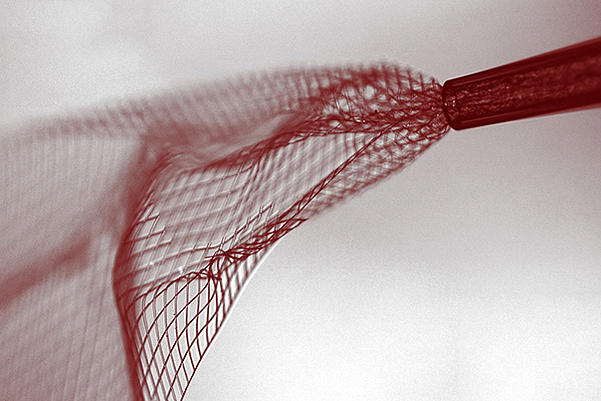
The process for fabricating the scaffolds is similar to that used to etch microchips, and begins with a dissolvable layer deposited on a substrate. To create the scaffold, researchers lay out a mesh of nanowires sandwiched in layers of organic polymer. The first layer is then dissolved, leaving the flexible mesh, which can be drawn into a needle and administered like any other injection.

The input-output of the mesh can then be connected to standard measurement electronics so that the integrated devices can be addressed and used to stimulate or record neural activity.

“These type of things have never been done before, from both a fundamental neuroscience and medical perspective,” Lieber said. “It’s really exciting — there are a lot of potential applications.”

Going forward, researchers hope to better understand how the body reacts to the injectable electronics over longer periods.

Harvard’s Office of Technology Development has filed for a provisional patent on the technology and is actively seeking commercialization opportunities.

“The idea of being able to precisely position and record from very specific areas, or even from specific neurons over an extended period of time — this could, I think, make a huge impact on neuroscience,” Lieber said.

Source: http://www.nanotechnologyworld.org/#!Injectable-electronics-promise-sharper-view-of-brain/c89r/5575efe90cf219f1772f8682