Showing posts with label crystal lattice. Show all posts

Tuesday, September 29, 2015

Computing A Textbook of Crystal Physics

Berkeley Lab scientists publish world’s largest database of piezoelectric properties


Disturbing a material’s crystal lattice can create a charge imbalance that leads to a voltage across the material. This phenomena, called the “piezoelectric effect,” was first demonstrated in 1880 by Jacques and Pierre Curie in materials such as quartz, topaz and Rochelle salt. Today, piezoelectricity is recognized as a valuable property and the market for piezoelectric materials is rapidly expanding with applications that encompass a variety of technologies, ranging from medical imaging to sonar to energy harvesting.
Despite its rising technological importance, the piezoelectric effect has been measured in only a handful of materials, but this is about to change. Researchers at Berkeley Lab and the University of California (UC) Berkeley have developed a methodology that enabled them to compute piezoelectric constants for nearly 1,000 inorganic compounds.
“People know how to calculate piezoelectric tensors but now we’ve developed a robust workflow for these calculations, which provides an unprecedented scaling of methodology for testing materials,” says Kristin Persson, staff scientist at Berkeley Lab’s Materials Sciences Division and leader of the Materials Project, which provides open web-based access to computed information on known and predicted materials. “Not only does this provide new open-access data to the community, but also indicates what structures and elements might be important for developing novel materials with strong piezoelectric properties.”
Kristin Persson leads the Materials Project, which provides open web-based access to computed information on known and predicted materials. (Photo by Roy Kaltschmidt)
In the new high-throughput calculations using the computing resources at the National Energy Research Scientific Computing Center (NERSC), hundreds of structures can be computed simultaneously. Compared to conventional experimental measurements, which could take years to cover the same number of materials, the “computational characterization” quickly identifies promising inorganic compounds in the Materials Project database that have the possibility of exhibiting piezoelectric behavior.
Persson, along with Mark Asta, staff scientist at Berkeley Lab and professor in UC Berkeley’s Department of Materials Science and Engineering, are co-authors of a paper describing this research in the journal Scientific Data. The paper is titled “A database to enable discovery and design of piezoelectric materials.” The other authors are Maarten de Jong, Wei Chen and   Henry Geerlings.
Certain structures of elements give rise to large piezoelectric responses: when subjected to a stress, they develop a stronger electric field. The larger the response – indicated by the tensor – the better the piezoelectric performance.
“The new database …will be invaluable for guiding the discovery of new candidate materials featuring enhanced performance, lower cost, and or more environmentally friendly constituents,” Asta says.
“We don’t collect experimental data – but we compare calculations with reported experimental piezoelectric constants,” says Persson. “For new materials that have not been measured before, it’s up to the community to test the data – by growing a film or a single crystal – and comparing with Materials Project computations.”
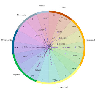
In 1910, Woldemar Voigt published the Textbook on Crystal Physics, defining the piezoelectric constants of 20 natural crystal classes. Now, the Materials Project has published tensor analyses that suggest completely new materials as potential piezoelectrics.
“The highest performing piezoelectric ceramics currently available contain high concentrations of lead, and significant efforts are aimed at identifying new lead-free compounds,” Asta says. “The new database is anticipated to greatly accelerate such materials discovery efforts.”
This research was funded by the Materials Project Center and made use of resources of the National Energy Research Scientific Computing Center (NERSC), supported by the Office of Basic Energy Sciences of the US Department of Energy.

Monday, February 24, 2014

On the road to Mottronics

Epitaxial mismatches in the lattices of nickelate
ultra-thin films can be used to tune the energetic
landscape of Mott materials and thereby control
conductor/insulator transitions.

Researchers at the Advanced Light Source Find Key to Controlling the Electronic and Magnetic Properties of Mott Thin Films


“Mottronics” is a term seemingly destined to become familiar to aficionados of electronic gadgets. Named for the Nobel laureate   Nevill Francis Mott, Mottronics involve materials – mostly metal oxides – that can be induced to transition between electrically conductive and insulating phases. If these phase transitions can be controlled, Mott materials hold great promise for future transistors and memories that feature higher energy efficiencies and faster switching speeds than today’s devices. A team of researchers working at Berkeley Lab’s Advanced Light Source (ALS) have  demonstrated the conducting/insulating phases of ultra-thin films of Mott materials can be controlled by applying an epitaxial strain to the crystal lattice.

“Our work shows how an epitaxial mismatch in the lattice can be used as a knot to tune the energetic landscape of Mott materials and thereby control conductor/insulator transitions,” says Jian Liu, a post-doctoral scholar now with Berkeley Lab’s Materials Sciences Division, who is the lead author on a paper describing this work in the journal Nature Communications. “Through epitaxial strain, we forced nickelate films containing only a few atomic layers into different phases with dramatically different electronic and magnetic properties. While some of these phases are not obtainable in conventional ways, we were able to produce them in a form that is ready for device development.”

The Nature Communications paper is titled “Heterointerface engineered electronic and magnetic phases of NdNiO3 thin films.” The corresponding author is Jak Chakhalian, a professor of physics at the University of Arkansas. Co-authors are Mehdi Kargarian, Mikhail Kareev, Ben Gray, Phil Ryan, Alejandro Cruz, Nadeem Tahir, Yi-De Chuang, Jinghua Guo, James Rondinelli, John Freeland and Gregory Fiete.

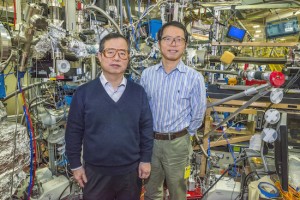
Jinghua Guo (left) and Yi-De Chuang at Beamline 8.0.1 of the Advanced Light Source were part of a team that discovered a key to controlling the electronic and magnetic properties of Mott materials. (Photo by Roy Kaltschmidt)
Nickel-based rare-earth perovskite oxides, or “nickelates,” are considered to be an ideal model for the study of Mott materials because they display strongly correlated electron systems that give rise to unique electronic and magnetic properties. Liu and his co-authors studied thin films of neodymium nickel oxide using ALS beamline 8.0.1, a high flux undulator beamline that produces x-ray beams optimized for the study of nanoscale materials and strongly correlated physics.

“ALS beamline 8.0.1 provides the high photon flux and energy range that are critical when dealing with nanoscale samples,” Liu says. “The state-of-the-art Resonant X-ray Scattering endstation has a high-speed, high-sensitivity CCD camera that makes it feasible to find and track diffraction peaks off a thin film that was only six nanometers thick.”

The transition between the conducting and insulating phases in nickelates is determined by various microscopic interactions, some of which favor the conducting phase, some which favor the insulating phase. The energetic balance of these interactions determines how easily electricity is conducted by electrons moving between the nickel and oxygen ions. By applying enough epitaxial strain to alter the space between these ions, Liu and his colleagues were able to tune this energetic balance and control the conducting/insulating transition. In addition, they   found strain could also be used to control the nickelate’s magnetic properties, again by exploiting the lattice mismatch.

“Magnetism is another hallmark of Mott materials that often goes hand-in-hand with the insulating state and is used to distinguish Mott insulators,” says Liu. “The challenge is that most Mott insulators, including nickelates, are antiferromagnets that macroscopically behave as non-magnetic materials. “At ALS beamline 8.0.1, we were able to directly track the magnetic evolution of our thin films while tuning the metal-to-insulator transition. Our findings give us a better understanding of the physics behind the magnetic properties of these nickelate films and point to potential applications for this magnetism in novel Mottronics devices.”
This research was primarily supported the U.S. Department of Energy’s Office of Science.

Source: http://newscenter.lbl.gov/science-shorts/2014/02/24/on-the-road-to-mottronics/