Showing posts with label nanometers. Show all posts

Monday, June 2, 2014

Rensselaer Researchers Predict the Electrical Response of Metals to Extreme Pressures


Findings Published in the Proceedings of the National Academy of Sciences Could Have Applications in Computer Chip Design

Research published today in the Proceedings of the National Academy of Sciences makes it possible to predict how subjecting metals to severe pressure can lower their electrical resistance, a finding that could have applications in computer chips and other materials that could benefit from specific electrical resistance. 

The semiconductor industry has long manipulated materials like silicon through the use of pressure, a strategy known as “strain engineering,” to improve the performance of transistors. But as the speed of transistors has increased, the limited speed of interconnects – the metal wiring between transistors – has become a barrier to increased computer chip speed. The published research paper, “Pressure Enabled Phonon Engineering in Metals,” opens the door to a new variant of strain engineering that can be applied to the metal interconnects, and other materials used to conduct or insulate electricity. “We looked at a fundamental physical property, the resistivity of a metal, and show that if you pressurize these metals, resistivity decreases. And not only that, we show that the decrease is specific to different materials – aluminum will show one decrease, but copper shows another decrease,” said Nicholas Lanzillo, a doctoral candidate at Rensselaer Polytechnic Institute and lead author on the study. 

“This paper explains why different materials see different decreases in these fundamental properties under pressure.” The research involved theoretical predictions, use of a supercomputer, and experimentation with equipment capable of exerting pressures up to 40,000 atmospheres (nearly 600,000 pounds per square inch). It was made possible through a collaboration between three Rensselaer professors – Saroj Nayak, a professor of physics, applied physics, and astronomy; Morris Washington, associate director of the Center for Materials, Devices, and Integrated Systems and professor of practice of physics, applied physics, and astronomy; and E. Bruce Watson, Institute Professor of Science, and professor of earth and environmental sciences and of materials science and engineering – with a diverse mix of disciplinary backgrounds and skill sets. Jay Thomas, a senior research scientist in Watson’s lab, was primarily responsible for designing the complex experiments detailed in the paper. When an electrical current is applied to metal, electrons travel through a lattice structure formed by the individual metal atoms, carrying the current along the wiring. But as an electron travels, it is impeded by the normal collective vibration of atoms in the lattice, which is one of the factors that leads to electrical resistance. In physics, the vibration is called phonon, and the resistance it creates by coupling with electrons is known as electron-phonon coupling, a quantum mechanical feature that amplifies strongly at the atomic scale. 

Lanzillo and Nayak, his doctoral adviser, said earlier research using the Center for Computational Innovations – the Rensselaer supercomputer – showed that electron phonon coupling varies depending on the scale of the wiring: nanoscale wire has typically higher resistance than ordinary size, or “bulk,” wiring. “Our goal was to understand what limits the resistivity, what accounts for the different resistance at the atomic scale,” said Nayak. “Our earlier findings showed that sometimes the resistance of the same metal in bulk and at the atomic scale could change by a factor of 10. That’s a big number in terms of resistivity.” The researchers wanted to conduct experiments to confirm their findings, but doing so would have required making atomic-scale wires, and measuring the electron-phonon coupling as a current passed through the wire, both difficult tasks. Then they saw an alternative, based on the observation that atoms were closer together in the atomic scale lattice than in bulk lattice. “We theorized that if we compress the bulk wire, we might be able to create a condition where the atoms are closer to each other, to mimic the conditions at the atomic scale,” said Nayak. They approached Watson and Washington to execute an experiment to test their finding. 

Washington and Nayak have long collaborated through the New York State Interconnect Focus Center at Rensselaer, which researches new material systems for the next generation of interconnects in semiconductor integrated circuits with a strong interest in interconnects at dimensions of less than 20 nanometers. Existing experimental data indicated that the resistivity of copper – the current preferred interconnect material – increases as the wiring size dips below 50 nanometers. One goal of the center is to suggest materials and structures for integrated circuit interconnects smaller than 20 nanometers, which often involves fabricating and characterizing experimental thin film structures with the resources of the Rensselaer Micro and Nano Fabrication Clean Room. With this background, Washington was critical to coordinating the experimental research. 

To pressurize the metals, the group turned to Watson, a geochemist who routinely subjects materials to enormous pressures to simulate conditions in the depths of the Earth. Watson had never experimented with the electrical properties of metal wires under pressure – a process that posed a number of technical challenges. Nevertheless, he was intrigued by the theoretical findings, and he and Thomas worked together to design the high-pressure experiments that provided information on the electrical resistivity of aluminum and copper at pressures up to 20,000 atmospheres. Working together, the team was able to demonstrate that the theoretical calculations were correct. “The experimental results were vital to the study because they confirmed that Saroj and Nick’s quantum mechanical calculations are accurate – their theory of electron-phonon coupling was validated,” said Watson. “And I think we would all argue that theory backed up by experimental confirmation makes the best science.” The authors said the research offers a new and exciting capability to predict the response of the resistivity to pressure through computer simulations. The research demonstrates that changes in resistivity can be achieved in thin film nanowires by using strain in combination with existing semiconductor wafer fabrication techniques and material. 

Because of this work, the physical properties and performance of a large number of metals can be further explored in a computer, saving time and expense of wafer fabrication runs. Lanzillo said the results are a complete package. “We can make this prediction with a computer simulation but it’s much more salient if we can get experimental confirmation,” said Lanzillo. “If we can go to a lab and actually take a block of aluminum and a block of copper and pressurize them and measure the resistivity. And that’s what we did. We made the theoretical prediction, and then our friends and colleagues in experiment are able to verify it in the lab and get quantitatively accurate results in both.” Funding for the research was partially supported by the National Science Foundation Integrative Graduate Education in Research and Traineeship (IGERT) Fellowship, Grant No. 0333314, as well as the Interconnect Focus Center (MARCO program) of New York state. Computing resources provided by the Center for Computational Innovations at Rensselaer, partly funded by the state of New York.

Source: http://news.rpi.edu/content/2014/06/02/rensselaer-researchers-predict-electrical-response-metals-extreme-pressures


Friday, March 14, 2014

Nanoscale optical switch breaks miniaturization barrier


An ultra-fast and ultra-small optical switch has been invented that could advance the day when photons replace electrons in the innards of consumer products ranging from cell phones to automobiles.
The new optical device can turn on and off trillions of times per second. It consists of individual switches that are only one five-hundredth the width of a human hair (200 nanometers) in diameter. This size is much smaller than the current generation of optical switches and it easily breaks one of the major technical barriers to the spread of electronic devices that detect and control light: miniaturizing the size of ultrafast optical switches.
Richard Haglund portrait
Physicist Richard Haglund has been studying the properties of vanadium dioxide for more than 20 years. (Joe Howell / Vanderbilt)
The new device was developed by a team of scientists from Vanderbilt University, University of Alabama-Birmingham, and Los Alamos National Laboratory and is described in the March 12 issue of the journal Nano Letters.
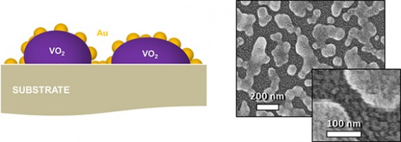
The ultrafast switch is made out of an artificial material engineered to have properties that are not found in nature. In this case, the “metamaterial” consists of nanoscale particles of vanadium dioxide (VO2) – a crystalline solid that can rapidly switch back and forth between an opaque, metallic phase and a transparent, semiconducting phase – which are deposited on a glass substrate and coated with a “nanomesh” of tiny gold nanoparticles.
The scientists report that bathing these gilded nanoparticles with brief pulses from an ultrafast laser generates hot electrons in the gold nanomesh that jump into the vanadium dioxide and cause it to undergo its phase change in a few trillionths of a second.
“We had previously triggered this transition in vanadium dioxide nanoparticles directly with lasers and we wanted to see if we could do it with electrons as well,” said Richard Haglund, Stevenson Professor of Physics at Vanderbilt, who led the study. “Not only does it work, but the injection of hot electrons from the gold nanoparticles also triggers the transformation with one fifth to one tenth as much energy input required by shining the laser directly on the bare VO2.”
Optical switch illustrations
Left: Illustration of terahertz optical switches shows the vanadium dioxide nanoparticles coated with a "nanomesh" of smaller gold particles. Right: Scanning electron microscope image of the switches at two resolutions. (Haglund Lab / Vanderbilt)
Both industry and government are investing heavily in efforts to integrate optics and electronics, because it is generally considered to be the next step in the evolution of information and communications technology. Intel, Hewlett-Packard and IBM have been building chips with increasing optical functionality for the last five years that operate at gigahertz speeds, one thousandth that of the VO2 switch.
“Vanadium dioxide switches have a number of characteristics that make them ideal for optoelectronics applications,” said Haglund. In addition to their fast speed and small size, they:
  • Are completely compatible with current integrated circuit technology, both silicon-based chips and the new “high-K dielectric” materials that the semiconductor industry is developing to continue the miniaturization process that has been a major aspect of microelectronics technology development;
  • Operate in the visible and near-infrared region of the spectrum that is optimal for telecommunications applications;
  • Generate an amount of heat per operation that is low enough so that the switches can be packed tightly enough to make practical devices: about ten trillionths of a calorie (100 femtojoules) per bit.
“Vanadium dioxide’s amazing properties have been known for more than half a century. At Vanderbilt, we have been studying VO2 nanoparticles for the last ten years, but the material has been remarkably successfully at resisting theoretical explanations,” said Haglund. “It is only in the last few years that intensive computational studies have illuminated the physics that underlies its semiconductor-to-metal transition.”
Student in clean room
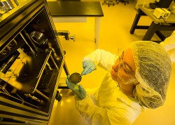
Graduate student Christina McGahan holding a disk on which centimeter square samples are grown. (Joe Howell / Vanderbilt)
Vanderbilt graduate students Kannatassen Appavoo and Joyeeta Nag fabricated the metamaterial at Vanderbilt; Appavoo joined forces with University of Alabama, Birmingham graduate student Nathaniel Brady and Professor David Hilton to carry out the ultrafast laser experiments with the guidance of Los Alamos National Laboratory staff scientist Rohit Prasankumar and postdoctoral scholar Minah Seo. The theoretical and computational studies that helped to unravel the complex mechanism of the phase transition at the nanoscale were carried out by postdoctoral student Bin Wang and Sokrates Pantelides, University Distinguished Professor of Physics and Engineering at Vanderbilt.
The university researchers were supported by Defense Threat-Reduction Agency grant HDTRA1-0047, U.S. Department of Energy grant DE-FG02-01ER45916, U.S. Department of Education GAANN Fellowship P200A090143 and National Science Foundation grant DMR-1207241. Portions of the research were performed at the Vanderbilt Institute of Nanoscale Science and Engineering in facilities renovated with NSF grant ARI-R2 DMR-0963361, at the Center for Integrated Nanotechnologies at Los Alamos National Laboratory under USDOE contract DE-AC52-06NA25396) and at Sandia National Laboratories under USDOE contract DE-AC04-94AL85000).
Source: http://news.vanderbilt.edu/2014/03/nanoscale-optical-switch/

Monday, October 28, 2013

Traces of DNA exposed by twisted light

Structures that put a spin on light reveal tiny amounts of DNA with 50 times better sensitivity than the best current methods, a collaboration between the University of Michigan and Jiangnan University in China has shown.
Highly sensitive detection of DNA can help with diagnosing patients, solving crimes and identifying the origins of biological contaminants such as a pathogen in a water supply.
"It really does not matter where the target DNA is from," said Nicholas Kotov, the Joseph B. and Florence V. Cejka Professor of Chemical Engineering at U-M. "In order to detect a specific DNA, we just need to know a small portion of its sequence."
Current DNA analysis methods rely on copying segments of a strand of DNA. The process unzips the double helix and then short, lab-made 'primer' DNA strands attach to each half of the original DNA. These primers kick-start the copying process, using the unzipped DNA as a template. Targeted segments of DNA can be replicated in this way, doubling every cycle. If enough DNA is produced before copying errors become a major problem, then further analysis can show whether the sample matches a suspect, for example.
But if the primers were very selective for the suspected DNA sequence, then a match could be determined by simply detecting whether the DNA had copied or not. Studies revealed that small amounts of DNA could be observed when spherical gold nanoparticles were attached to the primers. If the DNA matched suspicions, strings of particles bound together with DNA would form in the replication process. The nanoparticle solution would change color from red to blue, due to the way the strings of particles interact with light.
"Impressive detection limits were attained for short DNAs with nanoparticles; however, not for long DNA," Kotov said.
The problem, he explained, is that if the particles are further apart than a few nanometers, or millionths of a millimeter, "they do not interact strongly and the blue color does not happen." Longer strands are needed to differentiate between species and individuals with greater accuracy.
"If the strands are too short, you could mix up the DNA of a killer with that of the friend's dog—or a signature of malignant stomach cancer with the piece of a chicken burrito," Kotov said.
He and his partner Chuanlai Xu, a professor of food science and technology at Jiangnan University in China, led an effort to see whether a more subtle optical change would hold up to longer distances.
Rather than using spherical nanoparticles, the team started with nanorods, shaped like tiny Mike and Ike candies, about 62 nanometers long and 22 nanometers in diameter. They attached the primer DNA to the sides of these.
When nanorods line up, they tend to misalign by about 10 degrees. After a few rounds of copying, the gold and DNA structures resembled twisted rope ladders. Light passing through the spiral of golden spokes reacted by rotating.
"The light can be rotated even when the nanorods are far away from each other," Kotov said. "This gives our methods a tremendous advantage in sensitivity for long DNA strands."
The rotation happens because light is composed of electric and magnetic waves moving in tandem, and electric and magnetic fields exert forces on charged particles that have freedom to move, such as electrons in metals. The electrons in gold respond very well to the frequency of visible light waves, so they begin to move back and forth in the gold, synced with the light. This effect is a two-way street: the moving electrons in the gold can also affect the light waves.
Kotov compares the light to a rope with ripples running through it.
"Now imagine that the air around the rope can move more easily along certain directions," Kotov said.
For light passing through the gold nanorods, it's easiest if the electric wave moves up and down the length of the nanorods, so the light rotates as it moves from nanorod to nanorod and continues twisting after it leaves the structure. And depending on whether the light starts out rotating clockwise or counterclockwise, it feels the twist from the nanorods most at different wavelengths.
"For analytical purposes, this is a gift," Kotov said.
The two peaks in the amount of twisting for clockwise and counterclockwise light can be added together, which makes for a stronger signal and allows the method to identify a match with smaller amounts of DNA.
"The strength of the rotation reaches maximum when the gap between nanorods is 20 nanometers, which is exactly what we need for the detection of long, selective and species-specific DNA strands," Kotov said. "The calculations presented show that we can potentially increase the sensitivity even more in the future and to even longer DNAs."
The paper, "Attomolar DNA detection with Chiral Nanorod Assemblies," will be published in Nature Communications on Oct. 28. Kotov is a professor of chemical engineering, biomedical engineering, materials science and engineering, and macromolecular science and engineering.
This work was funded by the U.S. Department of Energy and National Science Foundation, National Natural Science Foundation of China, China Ministry of Science and Technology, and grants from the Ministries of Finance and Education in Jiangsu Province, China.

Monday, August 26, 2013

Size Matters as Nanocrystals Go Through Phases

Berkeley Lab Researchers at the Molecular Foundry Reveal Fundamental Size-Dependence of Metal Nanocrystals Undergoing Phase Transitions

Understanding what happens to a material as it undergoes phase transformations – changes from a solid to a liquid to a gas or a plasma – is of fundamental scientific interest and critical for optimizing commercial applications. For metal nanocrystals, assumptions about the size-dependence of phase transformations were made that now need to be re-evaluated. A team of researchers at the U.S. Department of Energy (DOE)’s Lawrence Berkeley National Laboratory (Berkeley Lab) has demonstrated that as metal nanocrystals go through phase transformations, size can make a much bigger difference than previously believed.

Working at Berkeley Lab’s Molecular Foundry, a DOE Nanoscale Science Research Center, the team led by Jeffrey Urban and Stephen Whitelam developed a unique optical probe based on luminescence that provided the first direct observations of metal nanocrystals undergoing phase transformations during reactions with hydrogen gas. Analysis of their observations revealed a surprising degree of size-dependence when it comes to such critical properties as thermodynamics and kinetics. These results hold important implications for the future design of hydrogen storage systems, catalysts, fuel cells and batteries.
“No one has ever directly observed phase transformations in metal nanocrystal systems before so no one saw the size dependence factor, which was obscured by other complicating effects, hidden in plain sight if you will,” Urban says. “The assumption had been that for nanocrystals beyond 15 nanometers, the thermodynamic and kinetic behavior would be essentially bulk-like. However, our results show that pure size effects can be understood and productively employed over a much broader range of nanocrystal sizes than previously thought.”
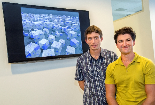
Stephen Whitelam (left) and Jeffrey Urban at Berkeley Lab’s Molecular Foundry led the first direct observations of metal nanocrystals undergoing phase transformations during reactions with hydrogen gas. (Photo by Roy Kaltschmidt)
Urban and Whitelam, both of whom hold appointments with Berkeley Lab’s Materials Sciences Division, are the corresponding authors of a paper describing this study in the journal Nature Materials. The paper is titled “Uncovering the intrinsic size dependence of hydriding phase transformations in nanocrystals.” Co-authors are Rizia Bardhan, Lester Hedges, Cary Pint and Ali Javey.
While it is well established that materials on the nanoscale can offer physical, chemical and mechanical properties not displayed at the microscale, knowledge as to how these properties can be altered as nanocrystals undergo phase transformations has been lacking.
“Quantitative understanding of nanocrystal phase transformations has been hindered by difficulties in directly monitoring well-characterized nanoscale systems in reactive environments,” Urban says.
Urban and his colleagues addressed this problem with a custom-built stainless steel gas-tight cell with optical windows and heating elements and connected to a high vacuum pump. They used this experimental setup to collect in situ luminescence spectra with a confocal Raman microscope as palladium nanocubes interacted with hydrogen gas. The nanocubes were synthesized by wet-chemistry and were all clear-faceted single-crystalline objects with a narrow range in size distribution.
“Our experimental setup allowed for rapid, direct monitoring of minuscule alterations in luminescence during hydrogen sorption,” Urban says. “This allowed us to uncover the size-dependence of the intrinsic thermodynamics and kinetics of hydriding and dehydriding phase transformations. We observed a dramatic decrease in luminescence as the palladium nanocubes formed hydrides. This lost luminescence was regained during dehydriding.”
This scanning electron micrograph shows palladium nanocubes with a side length of approximately 32 nanometers.
A statistical mechanical model whose development was led by Whitelam and co-author Hedges was then used to quantify the observational data for palladium nanocubes of all sizes. Because of the narrow size distribution of the nanocubes, Whitelam, Urban and their colleagues were able to show a direct correlation between luminescence and phase transitions that can be applied to other metal nanocrystal systems as well.
“Simple geometric arguments tell us that under certain conditions, thermally driven solid-state phase transformations are governed by nanocrystal dimensions,” Whitelam says. “These arguments further suggest ways of optimizing hydrogen storage kinetics in a variety of metal nanocrystal systems.”
The next step in this research will be to examine the effects of dopants on phase transformations in metal nanosystems.
“Our luminescence-probe and statistical mechanical model are a versatile combination,” Urban says, “that allow us to look at a number of gas-nanocrystal interactions in which controlling the thermodynamics of the interactions is paramount.”
This research was supported by DOE’s Office of Science through the Molecular Foundry and through the Center for Nanoscale Control of Geologic Carbon Dioxide, a DOE Energy Frontier Research Center. Additional support was provided by DOE’s Office of Energy Efficiency and Renewable Energy and by Mohr Davidow Ventures, a venture capital firm.
#  #  #
Lawrence Berkeley National Laboratory addresses the world’s most urgent scientific challenges by advancing sustainable energy, protecting human health, creating new materials, and revealing the origin and fate of the universe. Founded in 1931, Berkeley Lab’s scientific expertise has been recognized with 13 Nobel prizes. The University of California manages Berkeley Lab for the U.S. Department of Energy’s Office of Science. For more, visit www.lbl.gov.
The Molecular Foundry is one of five DOE Nanoscale Science Research Centers (NSRCs), national user facilities for interdisciplinary research at the nanoscale, supported by the DOE Office of Science.  Together the NSRCs comprise a suite of complementary facilities that provide researchers with state-of-the-art capabilities to fabricate, process, characterize and model nanoscale materials, and constitute the largest infrastructure investment of the National Nanotechnology Initiative.  The NSRCs are located at DOE’s Argonne, Brookhaven, Lawrence Berkeley, Oak Ridge and Sandia and Los Alamos National Laboratories.  For more information about the DOE NSRCs, please visit http://science.energy.gov.
The DOE Office of Science is the single largest supporter of basic research in the physical sciences in the United States and is working to address some of the most pressing challenges of our time. For more information, please visit science.energy.gov.