Showing posts with label nanostructure. Show all posts

Monday, April 14, 2014

New Physical Phenomenon on Nanowires Seen for the First Time

False-colour scanning electron micrograph of a nanowire strain device.
Very tiny wires made of semiconducting materials – more than one thousand times thinner than a human hair – promise to be an essential component for the semiconductor industry. Thanks to these tiny nanostructures, scientists envision not only a more powerful new generation of transistors, but also to integrate optical communication systems within the very same piece of silicon. This would make possible data transfer between chips at the speed of light.

But for optical communication to happen, it is essential to convert the electrical information used in the microprocessor into light, by using light emitters. On the other end of the optical link, one needs to translate the information contained in the stream of light into electrical signals by using light detectors. Current technologies use different materials to realize these two distinct functions – silicon or germanium for light detection and materials combining elements from the III-V columns of the periodic table for light emission. However, this might be going to change soon thanks to a new discovery.

In a paper appearing today in the journal Nature Communications, scientists at IBM Research – Zurich and the Norwegian University of Science and Technology have demonstrated for the first time that both, efficient light emission and detection functionalities can be achieved in the very same nanowire material by applying mechanical strain. 

Using this new physical phenomenon, scientists might be able to integrate the light emitter and the detector functions in the very same material. This would drastically reduce the complexity of future silicon nanophotonic chips.

IBM scientist Giorgio Signorello explains, "When you pull the nanowire along its length, the nanowire is in a state that we call “direct bandgap” and it can emit light very efficiently; when instead you compress the length of the wire, its electronic properties change and the material stops emitting light. We call this state “pseudo-direct”: the III-V material behaves similarly to silicon or germanium and becomes a good light detector."

IBM Fellow Heike Riel comments, “These are unique and surprising properties and they all come from the fact that the atoms are located at very special positions within the nanowire. We call this crystal structure “Wurtzite”. This structure is possible only because the nanowire dimensions are so small. You cannot achieve the same properties at dimensions visible to the eye. This is a great example of the power of nanotechnology.”

This remarkable properties might find interesting applications also outside the field of optical communication.

For the scientific background read the Nature Communications paper titled "Inducing a Direct-to-Pseudodirect Bandgap Transition in Wurtzite GaAs Nanowires with Uniaxial Stress”, doi:10.1038/ncomms4655

http://ibmresearchnews.blogspot.ch/2014/04/new-physical-phenomenon-on-nanowires.html

Friday, March 14, 2014

Brighter inks, without pigment

Nanostructured capsules could bring about paints and electronic displays that never fade

These photonic microcapsules have been prepared to produce blue, green, and red structural colors and imaged using bright-field (top) and dark-field (bottom) optical microscopy. (Images courtesy of Jin-Gyu Park.)
Among the taxidermal specimens in Harvard’s Museum of Comparative Zoology, past centuries-old fur coats, arises a flicker of brilliant blue. This is the spangled cotinga. Surprisingly, the cotinga is about as old as everything in the room, but its color is still as dazzling as the day it was brought to the museum. The cotinga—or rather its feathers—achieve this effect through structural color.

A spangled cotinga, formerly on display at the Harvard Museum of Natural History. (Photo courtesy of Curious Expeditions/Flickr under Creative Commons license CC BY-NC-SA 2.0.)
Unlike color that we usually think of, which arises from paints and dyes absorbing certain wavelengths of light and reflecting the remainder, structural color is created when an object’s very nanostructure amplifies a specific wavelength. Cells in the cotinga’s feathers have a series of tiny pores spaced just right so that blues (and not much of anything else) are reflected back to our eyes. Because of this, if the feathers were thoroughly pulverized, the formation of pores and therefore the color would be lost. It also means that the same color could be produced from an entirely different material, if one could recreate the same pattern made by the feathers' pores.
Researchers led by Vinothan N. Manoharan at the Harvard School of Engineering and Applied Sciences want to recreate this effect, giving man-made materials structural color. Producing structural color is not easy, though; it often requires a material’s molecules to be in a very specific crystalline pattern, like the natural structure of an opal, which reflects a wide array of colors. But the pores on the cotinga’s feathers lack a regular order and are therefore a prime target for imitation.
Manoharan's lab has devised a system where microcapsules are filled with a disordered solution of even smaller particles suspended in water. When the microcapsule is partly dried out, it shrinks, bringing the particles closer and closer together. Eventually the average distance between all the particles will give rise to a specific reflected color from the capsule. Shrink the capsule a bit more, and they become another color, and then another.
“There’s an average distance between particles, even though there is no ordering in the particles. It’s that average distance that is important in determining the color,” says Manoharan, Gordon McKay Professor of Chemical Engineering and Professor of Physics at Harvard.
The findings have been published in the journal Angewandte Chemie.
A microcapsule shrinks as it dries, arriving at its final color. (Image courtesy of Jin-Gyu Park.)

The current project expands on research conducted at Yale University in 2009, which aimed to mimic the cotinga’s hue and showed that dried aggregates of solid particles could create blues. Jin-Gyu Park was a postdoctoral researcher there and is now a research associate in Manoharan’s group at Harvard SEAS, which specializes in the physics of colloidal suspensions. With Park as lead author, the new paper demonstrates the production of colors across the spectrum, and the new encapsulation system.
The tunable color capsules present interesting technological opportunities, says Manoharan. For example, a whole spectrum of new paints might be created using suspended capsules.
“Right now, the red dye carmine comes from an insect called a cochineal,” says Manoharan. “People would like to move away from that because it’s very labor-intensive, and getting that color involves harvesting a lot of insects.”
Rather than harvesting from nature or preparing specialty chemicals, one for each color, these capsules could provide a universal and direct path to any desired color.
The capsules might also offer a safety advantage. The reason for using natural dyes like carmine is that many synthetic dyes are toxic. The new color capsules can be made with particles of almost any material in the right structural formation, so toxicity can be easily avoided.
Most compelling of all, however, is that some structural colors found in nature can last indefinitely as long as the colored object remains intact.
“Most color you get in paints, coatings or cosmetics, even, comes from the selective absorption and reflection of light. What that means is that the material is absorbing some energy, and that means that over time, the material will fade,” says Manoharan.
The sun’s energy pummels the molecules in conventional pigments. Eventually, the molecules simply deteriorate and no longer absorb the colors they used to, leading to sun bleaching. Manoharan’s group is currently testing their innovation to see if it can create an effectively ageless color.
Electronic display technology—for example, e-readers—might also benefit from this advance. The microcapsules could be used in displays that create pixels with colored particles rather than LEDs, liquid crystals, or black-and-white “electronic ink.”
“We think it could be possible to create a full-color display that won’t fade over time,” says Manoharan. “The dream is that you could have a piece of flexible plastic that you can put graphics on in full color and read in bright sunlight.”
The Harvard Office of Technology Development has filed a provisional patent and is working with Manoharan’s lab to pursue the commercialization of the color capsule technology.
Manoharan’s and Park’s coauthors were Sofia Magkiriadou, a Ph.D. student in physics at the Harvard Graduate School of Arts and Sciences; Shin-Hyun Kim and Tae Min Choi at the Korea Advanced Institute of Science and Technology; and Young-Seok Kim at Korea Electronics Technology Institute.
This research was supported by an International Collaboration grant from the Ministry of Trade, Industry & Energy of Korea, and by the Harvard Materials Research Science and Engineering Center through the U.S. National Science Foundation (NSF). The work was performed in part at the NSF-supported Center for Nanoscale Systems at Harvard University.
Source: http://www.seas.harvard.edu/news/2014/03/brighter-inks-without-pigment

Friday, October 25, 2013

Making the transition to the quantum world visible

Saarbrücken physicist want to make the transition to the quantum world to see

New insights into the quantum world is to open a micro-laboratory of Theoretical physicist Frank Wilhelm-Mauch and his team have developed by the University of the Saarland as a mathematical model. 100 photons, with their complex quantum mechanical relationships ("entanglement") can be studied simultaneously in the test system, as much as ever. The researchers expect new insights about the quantum computer. As the world's first group they use for their method a metamaterial, a custom-made grid of nanostructures, the light more breaks than any natural substance. Their results are published in Physical Review Letters.
A car is at the same time in one place. This place is exactly determined as well as the speed of the car: In the world in which we live, our known laws of nature. But these laws - and thus the classical physics - come in sizes smaller than an atom to a limit. Quantum particles, also called photons, or light quanta, are simultaneously in several places plus different rates - apply the laws of the quantum world: From this point everything else is in the micro world. About this transition of the end "two worlds" in which the laws of nature and start quantum laws, is little known today. "The quantum world can not simply just vermessbare, large systems transfer," explains Frank Wilhelm-Mauch. 's also a theoretical physicist and his research group have developed mathematical methods, a micro-lab, which is similar to a piece of ordinary aerial cable, but it should make it possible to study the transition between the two worlds in a controllable system. "We expect that the quantum properties of a certain size weaker or even lost entirely will. To explore this transition and specifically to investigate the quantum state specifically, we provide with our innovative concept of a very large test system 100 distinguishable photons as the basis for measurements ready, and without that a photon is lost. The cable is made ​​of superconducting material and the tests are carried out at low temperatures, "explains Professor Wilhelm-Mauch. 

So far, such undertaking are lossy: From hundred photons can today with the existing methods in the end only one can be investigated. Since the photons occupy multiple states at the same time, a measurement is also when it is done, only a tiny part of a highly complex process: The measured value always describes only one of the states. "That's why we make our test system with 100 photons as large as possible today to investigate this highly entangled, so interwoven processes. The measurements thus allow a much more accurate view of the processes, "he explains. Researchers outsmart this, the laws of classical optics. They combine the quantum optics with so-called "left-handed media," and direct this light particles through a "metamaterial". Such a grid of nanostructures is where research in classical optics for some time, have a special ability: light falling on it, is more broken than in nature, ie, such as water. The angle of refraction of light can be influenced. Also, the LAP physicists have mathematically tailored such a grid for photons of microwave radiation, which is good enough for the first time quantum optical studies. It consists of a series connection of capacitors and coils minute. With this waveguide very many photons can be packed into the smallest space and out the cable. This, the researchers want to use for quantum-optical measurements. investigate the transition to the quantum world, in particular, is of interest for the researchers. The knowledge of this interface can make the knowledge about our world precisely because even - or especially - in this case the quantum have their effects. This opens up new possibilities would open about the quantum computer, "If we find out how big of a quantum system can be up to make it even follows quantum mechanical laws, we could make the storage capacity as large as possible," said Wilhelm-Mauch. The theoretical physicist researching the international research network "Scaleqit" the quantum computer has been developed for this highly efficient microwave detector that can detect photons with one hundred percent efficiency. Currently, scientists of the universities of Karlsruhe and Syracuse (USA) on the laboratory prototype. Original publication :Daniel Egger, Frank Wilhelm-Mauch: "Multimode Circuit Quantum Electrodynamics with hybrid metamaterial transmission lines," Phys. Rev. Lett. 111, 163601 (2013) doi: 10.1103/PhysRevLett.111.163601


Source: http://www.uni-saarland.de/nc/en/news/article/nr/9225.html

Monday, September 16, 2013

Invention jet prints nanostructures with self-assembling material

A multi-institutional team of engineers has developed a new approach to the fabrication of nanostructures for the semiconductor and magnetic storage industries. This approach combines top-down advanced ink-jet printing technology with a bottom-up approach that involves self-assembling block copolymers, a type of material that can spontaneously form ultrafine structures.
The team, consisting of nine researchers from the University of Illinois at Urbana-Champaign, the University of Chicago and Hanyang University in Korea, was able to increase the resolution of their intricate structure fabrication from approximately 200 nanometers to approximately 15 nanometers. A nanometer is a billionth of a meter, the width of a double-stranded DNA molecule.
The ability to fabricate nanostructures out of polymers, DNA, proteins and other “soft” materials has the potential to enable new classes of electronics, diagnostic devices and chemical sensors. The challenge is that many of these materials are fundamentally incompatible with the sorts of lithographic techniques that are traditionally used in the integrated circuit industry. 
Recently developed ultrahigh resolution ink-jet printing techniques have some potential, with demonstrated resolution down to 100-200 nanometers, but there are significant challenges in achieving true nanoscale dimension. “Our work demonstrates that processes of polymer self-assembly can provide a way around this limitation,” said John Rogers, the Swanlund Chair Professor in Materials Science and Engineering at Illinois.
Rogers and his associates report their findings in the September issue of Nature Nanotechnology. Combining jet printing with self-assembling block copolymers enabled the engineers to attain the much higher resolution, as suggested by lead author Serdar Onses, a postdoctoral scientist at Illinois. Onses earned his doctorate at the University of Wisconsin under Paul Nealey, now the Brady W. Dougan Professor in Molecular Engineering at UChicago and a co-author of the Nature Nanotechnology paper. “This concept turned out to be really useful,” Rogers said.
Engineers use self-assembling materials to augment traditional photolithographic processes that generate patterns for many technological applications. They first create either a topographical or chemical pattern using traditional processes. For the Nature Nanotechnology paper, this was done at imec in Belgium, an independent nanoelectronics research center. Nealey’s laboratory pioneered this process of directed self-assembly of block copolymers using chemical nanopatterns.

NEARING THE LIMITS

The resolution of the chemical pattern nears the current limit of traditional photolithography, noted Lance Williamson, a graduate student in molecular engineering at UChicago and co-author of the Nature Nanotechnology article. “Imec has the capability to perform the photolithography at this scale over large areas with high precision,” Williamson said.
Back at the University of Illinois, engineers place a block copolymer atop this pattern. The block copolymer self-organizes, directed by the underlying template to form patterns that are at much higher resolution than the template itself.
Previous work has focused on the deposition and assembly of uniform films on each wafer or substrate, resulting in patterns with essentially only one characteristic feature size and spacing between features. But practical applications may need block copolymers of multiple dimensions patterned or spatially placed over a wafer.
“This invention, to use inkjet printing to deposit different block copolymer films with high spatial resolution over the substrate, is highly enabling in terms of device design and manufacturing in that you can realize different dimension structures all in one layer,” Nealey said. “Moreover, the different dimension patterns may actually be directed to assemble with either the same or different templates in different regions.”

BENEFITS OF E-JET PRINTING

The advanced form of ink-jet printing the engineers use to locally deposit block copolymers is called electrohydrodynamic, or e-jet printing. It operates much like the ink-jet printers office workers use for printing on paper. “The idea is flow of materials from small openings, except e-jet is a special, high-resolution version of ink-jet printers that can print features down to several hundred nanometers,” Onses said. And because e-jet can naturally handle fluid inks, it is exceptionally well-suited for patterning solution suspensions of nanotubes, nanocrystals, nanowires and other types of nanomaterials.
“The most interesting aspect of this work is the ability to combine ‘top-down’ techniques of jet printing with ‘bottom-up’ processes of self-assembly, in a way that opens up new capabilities in lithography—applicable to soft and hard materials alike,” Rogers said.
“The opportunities are in forming patterned structures of nanomaterials to enable their integration into real devices. I am optimistic about the possibilities.”

Sourc: http://news.uchicago.edu/article/2013/09/16/invention-jet-prints-nanostructures-self-assembling-material?utm_source=feedburner&utm_medium=feed&utm_campaign=Feed%3A+UchicagoNews%2FStories%2FScienceMedicine+%28UChicago+News%3A+Stories+-+Science+%26+Medicine%29#sthash.d6bNCDC1.dpuf

Tuesday, September 3, 2013

Plastic – the new energy source

QUT's research to develop cheap plastic solar cells to charge mobile phones and other electronic devices has been boosted with the installation of one of the most powerful nanotechnology microscopes in the world.
The only one if its kind in Australia, the Zeiss Orion NanoFab enables researchers to examine natural or manmade structures in incredible detail, and will create new insights wherever it is applied.
By increasing the microscope beam current, researchers are able to etch away material to create patterns or structures with features of only a few nanometres. This is a tool that can write lines 100,000 times finer than the text on a printed page. Imagine War and Peace etched on the head of a pin - 200 times over.
QUT nanotechnology expert, Professor Nunzio Motta, said the new microscope complemented QUT's existing tunnelling microscope, the only one of its kind in Queensland, and would cement the university's place at the cutting edge of Australian nanotechnology research.
He said the super microscopes would be used to create new nanostructures which could be used in electronic devices, solar cells, gas sensors and for a range of other uses.
"At the moment plastic solar cells are quite inefficient and researchers around the world are trying to determine how to make the cells efficient and able to be commercialised," Professor Motta said.
"The advantages cheap solar cells would produce would be enormous.
"In the future plastic solar cells could generate enough energy not only to recharge the batteries of laptops and mobiles, but even to obtain power from canopies on parking areas which could be fed back into grids.
"They could even be developed as a clear film on glass windows to produce power."
Professor Motta is currently using the tunnelling microscope to improve plastic solar cells by mixing them with graphene, an atomic-scale honeycomb lattice made of carbon atoms. He has found that adding gold nano-particles traps light and improves efficiency.
"While it's difficult to put a timeframe on the development of efficient plastic solar cells, a five to ten year goal is probably not unrealistic," he said.
Professor Motta said his research team also hoped to create a new class of solar-powered nano-sensors capable of detecting pollution and monitoring the environment in remote areas.
He said nanoscale science was critical to the world's future economy as advances would transform a range of scientific and engineering disciplines.
Professor Motta said QUT was organizing NanoS-E3, an International Workshop and School on nanotechnology at Airlie Beach in September.
The initiative, in partnership with the Italian and Australian governments, will build on existing nanotechnology networks and foster new collaborations. In 2013, the workshop will also welcome scientists from France, Germany, Japan, Canada and the USA.

Monday, August 26, 2013

Size Matters as Nanocrystals Go Through Phases

Berkeley Lab Researchers at the Molecular Foundry Reveal Fundamental Size-Dependence of Metal Nanocrystals Undergoing Phase Transitions

Understanding what happens to a material as it undergoes phase transformations – changes from a solid to a liquid to a gas or a plasma – is of fundamental scientific interest and critical for optimizing commercial applications. For metal nanocrystals, assumptions about the size-dependence of phase transformations were made that now need to be re-evaluated. A team of researchers at the U.S. Department of Energy (DOE)’s Lawrence Berkeley National Laboratory (Berkeley Lab) has demonstrated that as metal nanocrystals go through phase transformations, size can make a much bigger difference than previously believed.

Working at Berkeley Lab’s Molecular Foundry, a DOE Nanoscale Science Research Center, the team led by Jeffrey Urban and Stephen Whitelam developed a unique optical probe based on luminescence that provided the first direct observations of metal nanocrystals undergoing phase transformations during reactions with hydrogen gas. Analysis of their observations revealed a surprising degree of size-dependence when it comes to such critical properties as thermodynamics and kinetics. These results hold important implications for the future design of hydrogen storage systems, catalysts, fuel cells and batteries.
“No one has ever directly observed phase transformations in metal nanocrystal systems before so no one saw the size dependence factor, which was obscured by other complicating effects, hidden in plain sight if you will,” Urban says. “The assumption had been that for nanocrystals beyond 15 nanometers, the thermodynamic and kinetic behavior would be essentially bulk-like. However, our results show that pure size effects can be understood and productively employed over a much broader range of nanocrystal sizes than previously thought.”
Stephen Whitelam (left) and Jeffrey Urban at Berkeley Lab’s Molecular Foundry led the first direct observations of metal nanocrystals undergoing phase transformations during reactions with hydrogen gas. (Photo by Roy Kaltschmidt)
Urban and Whitelam, both of whom hold appointments with Berkeley Lab’s Materials Sciences Division, are the corresponding authors of a paper describing this study in the journal Nature Materials. The paper is titled “Uncovering the intrinsic size dependence of hydriding phase transformations in nanocrystals.” Co-authors are Rizia Bardhan, Lester Hedges, Cary Pint and Ali Javey.
While it is well established that materials on the nanoscale can offer physical, chemical and mechanical properties not displayed at the microscale, knowledge as to how these properties can be altered as nanocrystals undergo phase transformations has been lacking.
“Quantitative understanding of nanocrystal phase transformations has been hindered by difficulties in directly monitoring well-characterized nanoscale systems in reactive environments,” Urban says.
Urban and his colleagues addressed this problem with a custom-built stainless steel gas-tight cell with optical windows and heating elements and connected to a high vacuum pump. They used this experimental setup to collect in situ luminescence spectra with a confocal Raman microscope as palladium nanocubes interacted with hydrogen gas. The nanocubes were synthesized by wet-chemistry and were all clear-faceted single-crystalline objects with a narrow range in size distribution.
“Our experimental setup allowed for rapid, direct monitoring of minuscule alterations in luminescence during hydrogen sorption,” Urban says. “This allowed us to uncover the size-dependence of the intrinsic thermodynamics and kinetics of hydriding and dehydriding phase transformations. We observed a dramatic decrease in luminescence as the palladium nanocubes formed hydrides. This lost luminescence was regained during dehydriding.”
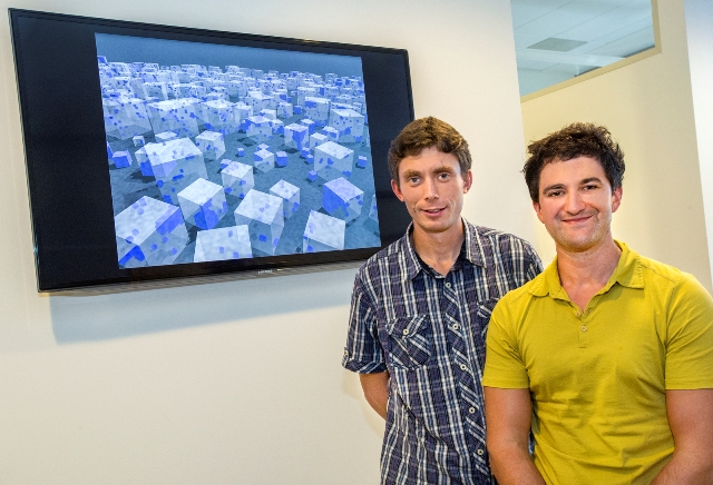
This scanning electron micrograph shows palladium nanocubes with a side length of approximately 32 nanometers.
A statistical mechanical model whose development was led by Whitelam and co-author Hedges was then used to quantify the observational data for palladium nanocubes of all sizes. Because of the narrow size distribution of the nanocubes, Whitelam, Urban and their colleagues were able to show a direct correlation between luminescence and phase transitions that can be applied to other metal nanocrystal systems as well.
“Simple geometric arguments tell us that under certain conditions, thermally driven solid-state phase transformations are governed by nanocrystal dimensions,” Whitelam says. “These arguments further suggest ways of optimizing hydrogen storage kinetics in a variety of metal nanocrystal systems.”
The next step in this research will be to examine the effects of dopants on phase transformations in metal nanosystems.
“Our luminescence-probe and statistical mechanical model are a versatile combination,” Urban says, “that allow us to look at a number of gas-nanocrystal interactions in which controlling the thermodynamics of the interactions is paramount.”
This research was supported by DOE’s Office of Science through the Molecular Foundry and through the Center for Nanoscale Control of Geologic Carbon Dioxide, a DOE Energy Frontier Research Center. Additional support was provided by DOE’s Office of Energy Efficiency and Renewable Energy and by Mohr Davidow Ventures, a venture capital firm.
#  #  #
Lawrence Berkeley National Laboratory addresses the world’s most urgent scientific challenges by advancing sustainable energy, protecting human health, creating new materials, and revealing the origin and fate of the universe. Founded in 1931, Berkeley Lab’s scientific expertise has been recognized with 13 Nobel prizes. The University of California manages Berkeley Lab for the U.S. Department of Energy’s Office of Science. For more, visit www.lbl.gov.
The Molecular Foundry is one of five DOE Nanoscale Science Research Centers (NSRCs), national user facilities for interdisciplinary research at the nanoscale, supported by the DOE Office of Science.  Together the NSRCs comprise a suite of complementary facilities that provide researchers with state-of-the-art capabilities to fabricate, process, characterize and model nanoscale materials, and constitute the largest infrastructure investment of the National Nanotechnology Initiative.  The NSRCs are located at DOE’s Argonne, Brookhaven, Lawrence Berkeley, Oak Ridge and Sandia and Los Alamos National Laboratories.  For more information about the DOE NSRCs, please visit http://science.energy.gov.
The DOE Office of Science is the single largest supporter of basic research in the physical sciences in the United States and is working to address some of the most pressing challenges of our time. For more information, please visit science.energy.gov.

Tuesday, August 20, 2013

‘Groovy’ hologram creates strange state of light at visible and invisible wavelengths

Nanostructured device controls the intensity, phase, and polarization of light for wide applications in optics
https://www.seas.harvard.edu/news/2013/08/groovy-hologram-creates-strange-state-of-light-at-visible-and-invisible-wavelengths Applied physicists at the Harvard School of Engineering and Applied Sciences (SEAS) have demonstrated that they can change the intensity, phase, and polarization of light rays using a hologram-like design decorated with nanoscale structures.
As a proof of principle, the researchers have used it to create an unusual state of light called a radially polarized beam, which—because it can be focused very tightly—is important for applications like high-resolution lithography and for trapping and manipulating tiny particles like viruses.
This is the first time a single, simple device has been designed to control these three major properties of light at once. (Phase describes how two waves interfere to either strengthen or cancel each other, depending on how their crests and troughs overlap; polarization describes the direction of light vibrations; and the intensity is the brightness.)
“Our lab works on using nanotechnology to play with light,” says Patrice Genevet, a research associate at Harvard SEAS and co-lead author of a paper published this month in Nano Letters. “In this research, we’ve used holography in a novel way, incorporating cutting-edge nanotechnology in the form of subwavelength structures at a scale of just tens of nanometers.” One nanometer equals one billionth of a meter.
Genevet works in the laboratory of Federico Capasso, Robert L. Wallace Professor of Applied Physics and Vinton Hayes Senior Research Fellow in Electrical Engineering at Harvard SEAS. Capasso’s research group in recent years has focused on nanophotonics—the manipulation of light at the nanometer scale—with the goal of creating new light beams and special effects that arise from the interaction of light with nanostructured materials.
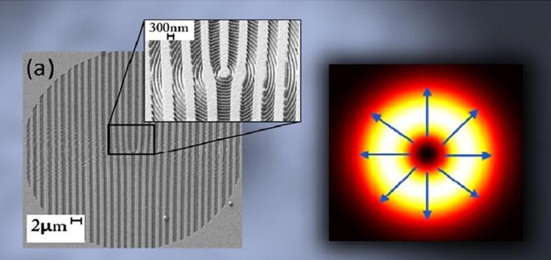
Left: holographic component fabricated by ion milling with a focused ion beam a 150-nanometer-thick gold film deposited on a glass substrate. A laser beam is partially transformed into a radially polarized beam as it traverses the device. The wide grooves create the donut-shaped intensity profile, known as a vortex, while the sub-wavelength nanometer grooves in the inset determine locally the radial polarization, which is perpendicular to the grooves. Right: The computed characteristic beam cross-section; the blue arrows indicate the radial polarization. (Image courtesy of Federico Capasso.)

Using these novel nanostructured holograms, the Harvard researchers have converted conventional, circularly polarized laser light into radially polarized beams at wavelengths spanning the technologically important visible and near-infrared light spectrum.
“When light is radially polarized, its electromagnetic vibrations oscillate inward and outward from the center of the beam like the spokes of a wheel,” explains Capasso. “This unusual beam manifests itself as a very intense ring of light with a dark spot in the center.”
“It is noteworthy,” Capasso points out, “that the same nanostructured holographic plate can be used to create radially polarized light at so many different wavelengths. Radially polarized light can be focused much more tightly than conventionally polarized light, thus enabling many potential applications in microscopy and nanoparticle manipulation.”
The new device resembles a normal hologram grating with an additional, nanostructured pattern carved into it. Visible light, which has a wavelength in the hundreds of nanometers, interacts differently with apertures textured on the ‘nano’ scale than with those on the scale of micrometers or larger. By exploiting these behaviors, the modular interface can bend incoming light to adjust its intensity, phase, and polarization.
Holograms, beyond being a staple of science-fiction universes, find many applications in security, like the holographic panels on credit cards and passports, and new digital hologram-based data-storage methods are currently being designed to potentially replace current systems. Achieving fine-tuned control of light is critical to advancing these technologies.
“Now, you can control everything you need with just a single interface,” says Genevet, pointing out that the polarization effect the new interface has on light could formerly only be achieved by a cascade of several different optical elements. “We’re gaining a big advantage in terms of saving space.”
The demonstration of this nanostructured hologram has become possible only recently with the development of more powerful software and higher resolution nanofabrication technologies.
The underlying design is more complex than a simple superposition of nanostructures onto the hologram. The phase and polarization of light closely interact, so the structures must be designed with both outcomes in mind, using modern computational tools.
Further research will aim to make more complex polarized holograms and to optimize the output efficiency of the device.
Genevet’s and Capasso’s collaborators included co-lead author Jiao Lin, a former SEAS postdoctoral fellow who is now at the Singapore Institute of Manufacturing Technology; Mikhail Kats, a graduate student at Harvard SEAS; and Nicholas Antoniou, principal focused ion beam engineer at the Center for Nanoscale Systems at Harvard University.
This research was supported in part by the Air Force Office of Scientific Research (FA9550-12-1-0289); the National Science Foundation (NSF), through a Graduate Research Fellowship; and the Agency for Science, Technology and Research (A*STAR) in Singapore. Device fabrication was carried out at the Center for Nanoscale Systems at Harvard University, which is a member of the NSF-supported National Nanotechnology Infrastructure Network (ECS-0335765).