Showing posts with label computer chips. Show all posts

Monday, February 1, 2016

Darwin on a chip


UT researchers develop (r)evolutionary circuits

Researchers of the MESA+ Institute for Nanotechnology and the CTIT Institute for ICT Research at the University of Twente in The Netherlands have demonstrated working electronic circuits that have been produced in a radically new way, using methods that resemble Darwinian evolution. The size of these circuits is comparable to the size of their conventional counterparts, but they are much closer to natural networks like the human brain. The findings promise a new generation of powerful, energy-efficient electronics, and have been published in the leading British journal Nature Nanotechnology.

One of the greatest successes of the 20th century has been the development of digital computers. During the last decades these computers have become more and more powerful by integrating ever smaller components on silicon chips. However, it is becoming increasingly hard and extremely expensive to continue this miniaturisation. Current transistors consist of only a handful of atoms. It is a major challenge to produce chips in which the millions of transistors have the same characteristics, and thus to make the chips operate properly. Another drawback is that their energy consumption is reaching unacceptable levels. It is obvious that one has to look for alternative directions, and it is interesting to see what we can learn from nature. Natural evolution has led to powerful ‘computers’ like the human brain, which can solve complex problems in an energy-efficient way. Nature exploits complex networks that can execute many tasks in parallel.

Moving away from designed circuits

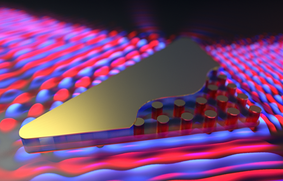
The approach of the researchers at the University of Twente is based on methods that resemble those found in Nature. They have used networks of gold nanoparticles for the execution of essential computational tasks. Contrary to conventional electronics, they have moved away from designed circuits. By using 'designless' systems, costly design mistakes are avoided. The computational power of their networks is enabled by applying artificial evolution. This evolution takes less than an hour, rather than millions of years. By applying electrical signals, one and the same network can be configured into 16 different logical gates. The evolutionary approach works around - or can even take advantage of - possible material defects that can be fatal in conventional electronics.

Powerful and energy-efficient

It is the first time that scientists have succeeded in this way in realizing robust electronics with dimensions that can compete with commercial technology. According to prof. Wilfred van der Wiel, the realized circuits currently still have limited computing power. “But with this research we have delivered proof of principle: demonstrated that our approach works in practice. By scaling up the system, real added value will be produced in the future. Take for example the efforts to recognize patterns, such as with face recognition. This is very difficult for a regular computer, while humans and possibly also our circuits can do this much better."  Another important advantage may be that this type of circuitry uses much less energy, both in the production, and during use. The researchers anticipate a wide range of applications, for example in portable electronics and in the medical world.

Monday, October 19, 2015

To infinity and beyond: Light goes infinitely fast with new on-chip material


Electrons are so 20th century. In the 21st century, photonic devices, which use light to transport large amounts of information quickly, will enhance or even replace the electronic devices that are ubiquitous in our lives today. But there’s a step needed before optical connections can be integrated into telecommunications systems and computers: researchers need to make it easier to manipulate light at the nanoscale.  

Researchers at the Harvard John A. Paulson School of Engineering and Applied Sciences (SEAS) have done just that, designing the first on-chip metamaterial with a refractive index of zero, meaning that the phase of light can travel infinitely fast. 

This new metamaterial was developed in the lab of Eric Mazur, the Balkanski Professor of Physics and Applied Physics and Area Dean for Applied Physics at SEAS, and is described in the journal Nature Photonics.

“Light doesn’t typically like to be squeezed or manipulated but this metamaterial permits you to manipulate light from one chip to another, to squeeze, bend, twist and reduce diameter of a beam from the macroscale to the nanoscale,” said Mazur. “It’s a remarkable new way to manipulate light.”

Although this infinitely high velocity sounds like it breaks the rule of relativity, it doesn’t. Nothing in the universe travels faster than light carrying information — Einstein is still right about that. But light has another speed, measured by how fast the crests of a wavelength move, known as phase velocity. This speed of light increases or decreases depending on the material it’s moving through.

When light passes through water, for example, its phase velocity is reduced as its wavelengths get squished together. Once it exits the water, its phase velocity increases again as its wavelength elongates. How much the crests of a light wave slow down in a material is expressed as a ratio called the refraction index — the higher the index, the more the material interferes with the propagation of the wave crests of light. Water, for example, has a refraction index of about 1.3.

When the refraction index is reduced to zero, really weird and interesting things start to happen.
In a zero-index material, there is no phase advance, meaning light no longer behaves as a moving wave, traveling through space in a series of crests and troughs. Instead, the zero-index material creates a constant phase — all crests or all troughs — stretching out in infinitely long wavelengths.  The crests and troughs oscillate only as a variable of time, not space.

This uniform phase allows the light to be stretched or squished, twisted or turned, without losing energy. A zero-index material that fits on a chip could have exciting applications, especially in the world of quantum computing.  

“Integrated photonic circuits are hampered by weak and inefficient optical energy confinement in standard silicon waveguides,” said Yang Li, a postdoctoral fellow in the Mazur Group and first author on the paper. “This zero-index metamaterial offers a solution for the confinement of electromagnetic energy in different waveguide configurations because its high internal phase velocity produces full transmission, regardless of how the material is configured.” 

The metamaterial consists of silicon pillar arrays embedded in a polymer matrix and clad in gold film. It can couple to silicon waveguides to interface with standard integrated photonic components and chips.

“In quantum optics, the lack of phase advance would allow quantum emitters in a zero-index cavity or waveguide to emit photons which are always in phase with one another,” said Philip Munoz, a graduate student in the Mazur lab and co-author on the paper.  “It could also improve entanglement between quantum bits, as incoming waves of light are effectively spread out and infinitely long, enabling even distant particles to be entangled.”

“This on-chip metamaterial opens the door to exploring the physics of zero index and its applications in integrated optics,” said Mazur. 

Friday, September 11, 2015

First new cache-coherence mechanism in 30 years


More efficient memory-management scheme could help enable chips with thousands of cores.


In a modern, multicore chip, every core — or processor — has its own small memory cache, where it stores frequently used data. But the chip also has a larger, shared cache, which all the cores can access.
If one core tries to update data in the shared cache, other cores working on the same data need to know. So the shared cache keeps a directory of which cores have copies of which data.
That directory takes up a significant chunk of memory: In a 64-core chip, it might be 12 percent of the shared cache. And that percentage will only increase with the core count. Envisioned chips with 128, 256, or even 1,000 cores will need a more efficient way of maintaining cache coherence.
At the International Conference on Parallel Architectures and Compilation Techniques in October, MIT researchers unveil the first fundamentally new approach to cache coherence in more than three decades. Whereas with existing techniques, the directory’s memory allotment increases in direct proportion to the number of cores, with the new approach, it increases according to the logarithm of the number of cores.
In a 128-core chip, that means that the new technique would require only one-third as much memory as its predecessor. With Intel set to release a 72-core high-performance chip in the near future, that’s a more than hypothetical advantage. But with a 256-core chip, the space savings rises to 80 percent, and with a 1,000-core chip, 96 percent.
When multiple cores are simply reading data stored at the same location, there’s no problem. Conflicts arise only when one of the cores needs to update the shared data. With a directory system, the chip looks up which cores are working on that data and sends them messages invalidating their locally stored copies of it.
“Directories guarantee that when a write happens, no stale copies of the data exist,” says Xiangyao Yu, an MIT graduate student in electrical engineering and computer science and first author on the new paper. “After this write happens, no read to the previous version should happen. So this write is ordered after all the previous reads in physical-time order.”
Time travel
What Yu and his thesis advisor — Srini Devadas, the Edwin Sibley Webster Professor in MIT’s Department of Electrical Engineering and Computer Science — realized was that the physical-time order of distributed computations doesn’t really matter, so long as their logical-time order is preserved. That is, core A can keep working away on a piece of data that core B has since overwritten, provided that the rest of the system treats core A’s work as having preceded core B’s.
The ingenuity of Yu and Devadas’ approach is in finding a simple and efficient means of enforcing a global logical-time ordering. “What we do is we just assign time stamps to each operation, and we make sure that all the operations follow that time stamp order,” Yu says.
With Yu and Devadas’ system, each core has its own counter, and each data item in memory has an associated counter, too. When a program launches, all the counters are set to zero. When a core reads a piece of data, it takes out a “lease” on it, meaning that it increments the data item’s counter to, say, 10. As long as the core’s internal counter doesn’t exceed 10, its copy of the data is valid. (The particular numbers don’t matter much; what matters is their relative value.)
When a core needs to overwrite the data, however, it takes “ownership” of it. Other cores can continue working on their locally stored copies of the data, but if they want to extend their leases, they have to coordinate with the data item’s owner. The core that’s doing the writing increments its internal counter to a value that’s higher than the last value of the data item’s counter.
Say, for instance, that cores A through D have all read the same data, setting their internal counters to 1 and incrementing the data’s counter to 10. Core E needs to overwrite the data, so it takes ownership of it and sets its internal counter to 11. Its internal counter now designates it as operating at a later logical time than the other cores: They’re way back at 1, and it’s ahead at 11. The idea of leaping forward in time is what gives the system its name — Tardis, after the time-traveling spaceship of the British science fiction hero Dr. Who.
Now, if core A tries to take out a new lease on the data, it will find it owned by core E, to which it sends a message. Core E writes the data back to the shared cache, and core A reads it, incrementing its internal counter to 11 or higher.
Unexplored potential
In addition to saving space in memory, Tardis also eliminates the need to broadcast invalidation messages to all the cores that are sharing a data item. In massively multicore chips, Yu says, this could lead to performance improvements as well. “We didn’t see performance gains from that in these experiments,” Yu says. “But that may depend on the benchmarks” — the industry-standard programs on which Yu and Devadas tested Tardis. “They’re highly optimized, so maybe they already removed this bottleneck,” Yu says.
“There have been other people who have looked at this sort of lease idea,” says Christopher Hughes, a principal engineer at Intel Labs, “but at least to my knowledge, they tend to use physical time. You would give a lease to somebody and say, ‘OK, yes, you can use this data for, say, 100 cycles, and I guarantee that nobody else is going to touch it in that amount of time.’ But then you’re kind of capping your performance, because if somebody else immediately afterward wants to change the data, then they’ve got to wait 100 cycles before they can do so. Whereas here, no problem, you can just advance the clock. That is something that, to my knowledge, has never been done before. That’s the key idea that’s really neat.”
Hughes says, however, that chip designers are conservative by nature. “Almost all mass-produced commercial systems are based on directory-based protocols,” he says. “We don’t mess with them because it’s so easy to make a mistake when changing the implementation.”
But “part of the advantage of their scheme is that it is conceptually somewhat simpler than current [directory-based] schemes,” he adds. “Another thing that these guys have done is not only propose the idea, but they have a separate paper actually proving its correctness. That’s very important for folks in this field.”

Tuesday, May 26, 2015

A new kind of biodegradable computer wood chip

A cellulose nanofibril (CNF) computer chip rests on a leaf. Photo: Yei Hwan Jung, Wisconsin Nano
Engineering Device Laboratory

Portable electronics — typically made of non-renewable, non-biodegradable and potentially toxic materials — are discarded at an alarming rate in consumers' pursuit of the next best electronic gadget.

In an effort to alleviate the environmental burden of electronic devices, a team of University of Wisconsin-Madison researchers has collaborated with researchers in the Madison-based U.S. Department of Agriculture Forest Products Laboratory (FPL) to develop a surprising solution: a semiconductor chip made almost entirely of wood.

The research team, led by UW-Madison electrical and computer engineering professor Zhenqiang "Jack" Ma, described the new device in a paper published today (May 26, 2015) by the journal Nature Communications. The paper demonstrates the feasibility of replacing the substrate, or support layer, of a computer chip, with cellulose nanofibril (CNF), a flexible, biodegradable material made from wood.

"The majority of material in a chip is support. We only use less than a couple of micrometers for everything else," Ma says. "Now the chips are so safe you can put them in the forest and fungus will degrade it. They become as safe as fertilizer."

Zhiyong Cai, project leader for an engineering composite science research group at FPL, has been developing sustainable nanomaterials since 2009.

"If you take a big tree and cut it down to the individual fiber, the most common product is paper. The dimension of the fiber is in the micron stage," Cai says. "But what if we could break it down further to the nano scale? At that scale you can make this material, very strong and transparent CNF paper."

"You don't want it to expand or shrink too much. Wood is a natural hydroscopic material and could attract moisture from the air and expand," Cai says. "With an epoxy coating on the surface of the CNF, we solved both the surface smoothness and the moisture barrier."Working with Shaoqin "Sarah" Gong, a UW-Madison professor of biomedical engineering, Cai's group addressed two key barriers to using wood-derived materials in an electronics setting: surface smoothness and thermal expansion.

Gong and her students also have been studying bio-based polymers for more than a decade. CNF offers many benefits over current chip substrates, she says.
"The advantage of CNF over other polymers is that it's a bio-based material and most other polymers are petroleum-based polymers. Bio-based materials are sustainable, bio-compatible and biodegradable," Gong says. "And, compared to other polymers, CNF actually has a relatively low thermal expansion coefficient."

The group's work also demonstrates a more environmentally friendly process that showed performance similar to existing chips. The majority of today's wireless devices use gallium arsenide-based microwave chips due to their superior high-frequency operation and power handling capabilities. However, gallium arsenide can be environmentally toxic, particularly in the massive quantities of discarded wireless electronics.

Yei Hwan Jung, a graduate student in electrical and computer engineering and a co-author of the paper, says the new process greatly reduces the use of such expensive and potentially toxic material.

"I've made 1,500 gallium arsenide transistors in a 5-by-6 millimeter chip. Typically for a microwave chip that size, there are only eight to 40 transistors. The rest of the area is just wasted," he says. "We take our design and put it on CNF using deterministic assembly technique, then we can put it wherever we want and make a completely functional circuit with performance comparable to existing chips."

While the biodegradability of these materials will have a positive impact on the environment, Ma says the flexibility of the technology can lead to widespread adoption of these electronic chips.

"Mass-producing current semiconductor chips is so cheap, and it may take time for the industry to adapt to our design," he says. "But flexible electronics are the future, and we think we're going to be well ahead of the curve."

Source: http://www.news.wisc.edu/23805

Monday, June 2, 2014

Rensselaer Researchers Predict the Electrical Response of Metals to Extreme Pressures


Findings Published in the Proceedings of the National Academy of Sciences Could Have Applications in Computer Chip Design

Research published today in the Proceedings of the National Academy of Sciences makes it possible to predict how subjecting metals to severe pressure can lower their electrical resistance, a finding that could have applications in computer chips and other materials that could benefit from specific electrical resistance. 

The semiconductor industry has long manipulated materials like silicon through the use of pressure, a strategy known as “strain engineering,” to improve the performance of transistors. But as the speed of transistors has increased, the limited speed of interconnects – the metal wiring between transistors – has become a barrier to increased computer chip speed. The published research paper, “Pressure Enabled Phonon Engineering in Metals,” opens the door to a new variant of strain engineering that can be applied to the metal interconnects, and other materials used to conduct or insulate electricity. “We looked at a fundamental physical property, the resistivity of a metal, and show that if you pressurize these metals, resistivity decreases. And not only that, we show that the decrease is specific to different materials – aluminum will show one decrease, but copper shows another decrease,” said Nicholas Lanzillo, a doctoral candidate at Rensselaer Polytechnic Institute and lead author on the study. 

“This paper explains why different materials see different decreases in these fundamental properties under pressure.” The research involved theoretical predictions, use of a supercomputer, and experimentation with equipment capable of exerting pressures up to 40,000 atmospheres (nearly 600,000 pounds per square inch). It was made possible through a collaboration between three Rensselaer professors – Saroj Nayak, a professor of physics, applied physics, and astronomy; Morris Washington, associate director of the Center for Materials, Devices, and Integrated Systems and professor of practice of physics, applied physics, and astronomy; and E. Bruce Watson, Institute Professor of Science, and professor of earth and environmental sciences and of materials science and engineering – with a diverse mix of disciplinary backgrounds and skill sets. Jay Thomas, a senior research scientist in Watson’s lab, was primarily responsible for designing the complex experiments detailed in the paper. When an electrical current is applied to metal, electrons travel through a lattice structure formed by the individual metal atoms, carrying the current along the wiring. But as an electron travels, it is impeded by the normal collective vibration of atoms in the lattice, which is one of the factors that leads to electrical resistance. In physics, the vibration is called phonon, and the resistance it creates by coupling with electrons is known as electron-phonon coupling, a quantum mechanical feature that amplifies strongly at the atomic scale. 

Lanzillo and Nayak, his doctoral adviser, said earlier research using the Center for Computational Innovations – the Rensselaer supercomputer – showed that electron phonon coupling varies depending on the scale of the wiring: nanoscale wire has typically higher resistance than ordinary size, or “bulk,” wiring. “Our goal was to understand what limits the resistivity, what accounts for the different resistance at the atomic scale,” said Nayak. “Our earlier findings showed that sometimes the resistance of the same metal in bulk and at the atomic scale could change by a factor of 10. That’s a big number in terms of resistivity.” The researchers wanted to conduct experiments to confirm their findings, but doing so would have required making atomic-scale wires, and measuring the electron-phonon coupling as a current passed through the wire, both difficult tasks. Then they saw an alternative, based on the observation that atoms were closer together in the atomic scale lattice than in bulk lattice. “We theorized that if we compress the bulk wire, we might be able to create a condition where the atoms are closer to each other, to mimic the conditions at the atomic scale,” said Nayak. They approached Watson and Washington to execute an experiment to test their finding. 

Washington and Nayak have long collaborated through the New York State Interconnect Focus Center at Rensselaer, which researches new material systems for the next generation of interconnects in semiconductor integrated circuits with a strong interest in interconnects at dimensions of less than 20 nanometers. Existing experimental data indicated that the resistivity of copper – the current preferred interconnect material – increases as the wiring size dips below 50 nanometers. One goal of the center is to suggest materials and structures for integrated circuit interconnects smaller than 20 nanometers, which often involves fabricating and characterizing experimental thin film structures with the resources of the Rensselaer Micro and Nano Fabrication Clean Room. With this background, Washington was critical to coordinating the experimental research. 

To pressurize the metals, the group turned to Watson, a geochemist who routinely subjects materials to enormous pressures to simulate conditions in the depths of the Earth. Watson had never experimented with the electrical properties of metal wires under pressure – a process that posed a number of technical challenges. Nevertheless, he was intrigued by the theoretical findings, and he and Thomas worked together to design the high-pressure experiments that provided information on the electrical resistivity of aluminum and copper at pressures up to 20,000 atmospheres. Working together, the team was able to demonstrate that the theoretical calculations were correct. “The experimental results were vital to the study because they confirmed that Saroj and Nick’s quantum mechanical calculations are accurate – their theory of electron-phonon coupling was validated,” said Watson. “And I think we would all argue that theory backed up by experimental confirmation makes the best science.” The authors said the research offers a new and exciting capability to predict the response of the resistivity to pressure through computer simulations. The research demonstrates that changes in resistivity can be achieved in thin film nanowires by using strain in combination with existing semiconductor wafer fabrication techniques and material. 

Because of this work, the physical properties and performance of a large number of metals can be further explored in a computer, saving time and expense of wafer fabrication runs. Lanzillo said the results are a complete package. “We can make this prediction with a computer simulation but it’s much more salient if we can get experimental confirmation,” said Lanzillo. “If we can go to a lab and actually take a block of aluminum and a block of copper and pressurize them and measure the resistivity. And that’s what we did. We made the theoretical prediction, and then our friends and colleagues in experiment are able to verify it in the lab and get quantitatively accurate results in both.” Funding for the research was partially supported by the National Science Foundation Integrative Graduate Education in Research and Traineeship (IGERT) Fellowship, Grant No. 0333314, as well as the Interconnect Focus Center (MARCO program) of New York state. Computing resources provided by the Center for Computational Innovations at Rensselaer, partly funded by the state of New York.

Source: http://news.rpi.edu/content/2014/06/02/rensselaer-researchers-predict-electrical-response-metals-extreme-pressures

Sunday, January 12, 2014

Designing the Next Wave of Computer Chips

Nanomaterials arranged on a chip before being cut into their final forms at the SLAC National Accelerator Laboratory in Menlo Park, Calif. Matt Beardsley/SLAC


Not long after Gordon E. Moore proposed in 1965 that the number of transistors that could be etched on a silicon chip would continue to double approximately every 18 months, critics began predicting that the era of “Moore’s Law” would draw to a close.

More than ever recently, industry pundits have been warning that the progress of the semiconductor industry is grinding to a halt — and that the theory of Dr. Moore, an Intel co-founder, has run its course.

If so, that will have a dramatic impact on the computer world. The innovation that has led to personal computers, music players and smartphones is directly related to the plunging cost of transistors, which are now braided by the billions onto fingernail slivers of silicon — computer chips — that may sell for as little as a few dollars each.

But Moore’s Law is not dead; it is just evolving, according to more optimistic scientists and engineers. Their contention is that it will be possible to create circuits that are closer to the scale of individual molecules by using a new class of nanomaterials — metals, ceramics, polymeric or composite materials that can be organized from the “bottom up,” rather than the top down.

For instance, semiconductor designers are developing chemical processes that can make it possible to “self assemble” circuits by causing the materials to form patterns of ultrathin wires on a semiconductor wafer. Combining these patterns of nanowires with conventional chip-making techniques, the scientists believe, will lead to a new class of computer chips, keeping Moore’s Law alive while reducing the cost of making chips in the future.

“The key is self assembly,” said Chandrasekhar Narayan, director of science and technology at IBM’s Almaden Research Center in San Jose, Calif. “You use the forces of nature to do your work for you. Brute force doesn’t work any more; you have to work with nature and let things happen by themselves.”

To do this, semiconductor manufacturers will have to move from the silicon era to what might be called the era of computational materials. Researchers here in Silicon Valley, using powerful new supercomputers to simulate their predictions, are leading the way. While semiconductor chips are no longer made here, the new classes of materials being developed in this area are likely to reshape the computing world over the next decade.

“Materials are very important to our human societies,” said Shoucheng Zhang, a Stanford University physicist who recently led a group of researchers to design a tin alloy that has superconductinglike properties at room temperature. “Entire eras are named after materials — the stone age, the iron age and now we have the silicon age. In the past they have been discovered serendipitously. Once we have the power to predict materials, I think it’s transformative.”

Pushing this research forward is economics — specifically, the staggering cost semiconductor manufacturers are expecting to pay for their next-generation factories. In the chip-making industry this has been referred to as “Moore’s Second Law.”

Two years from now new factories for making microprocessor chips will cost from $8 to $10 billion, according to a recent Gartner report — more than twice as much as the current generation. That amount could rise to between $15 and $20 billion by the end of the decade, equivalent to the gross domestic product of a small nation.

The stunning expenditures that soon will be required mean that the risk of error for chip companies is immense. So rather than investing in expensive conventional technologies that might fail, researchers are looking to these new self-assembling materials.

In December, researchers at Sandia National Laboratories in Livermore, Calif., published a Science paper describing advances in a new class of materials called “metal-organic frameworks” or MOFs. These are crystalline ensembles of metal ions and organic molecules. They have been simulated with high-performance computers, and then verified experimentally.

What the scientists have proven is that they can create conductive thin films, which could be used in a range of applications, including photovoltaics, sensors and electronic materials.

The scientists said that they now see paths for moving beyond the conductive materials, toward creating semiconductors as well.

According to Mark D. Allendorf, a Sandia chemist, there are very few things that you can do with conventional semiconductorsto change the behavior of a material. With MOFs he envisions a future in which molecules can be precisely ordered to create materials with specific behaviors.

“One of the reasons that Sandia is well positioned is that we have huge supercomputers,” he said. They have been able to simulate matrixes of 600 atoms, large enough for the computer to serve as an effective test tube.

In November, scientists at the SLAC National Accelerator Laboratory, writing in the journal Physical Review Letters, described a new form of tin that, at only a single molecule thick, has been predicted to conduct electricity with 100 percent efficiency at room temperature. Until now these kinds of efficiencies have only been found in materials known as superconductors, and then only at temperatures near absolute zero.

The material would be an example of a new class of materials called “topological insulators” that are highly conductive along a surface or edge, but insulating on their interior. In this case the researchers have proposed a structure with fluorine atoms added to a single layer of tin atoms.

The scientists, led by Dr. Zhang, named the new material stanene, combining the Latin name for tin — stannum — with the suffix used for graphene, another material based on a sheet of carbon atoms a single molecule thick.

The promise of such a material is that it might be easily used in conjunction with today’s chip-making processes to both increase the speed and lower the power consumption of future generations of semiconductors.

The theoretical prediction of the material must still be verified, and Dr. Zhang said that research is now taking place in Germany and China, as well as a laboratory at U.C.L.A.

It is quite possible that the computational materials revolution may offer a path toward cheaper technologies for the next generation of computer chips.

That is IBM’s bet. The company is now experimenting with exotic polymers that automatically form into an ultrafine web and can be used to form circuit patterns onto silicon wafers.

Dr. Narayan is cautiously optimistic, saying there is a good chance that bottoms-up self-assembly techniques will eliminate the need to invest in new lithographic machines, costing $500 million, that use X-rays to etch smaller circuits. .

“The answer is possibly yes,” he said, in describing a lower cost path to denser computer chips.