Showing posts with label photodetectors. Show all posts

Wednesday, January 20, 2016

Watching Electrons Cool in 30 Quadrillionths of a Second


Two University of California, Riverside assistant professors of physics are among a team of researchers that have developed a new way of seeing electrons cool off in an extremely short time period.

The development could have applications in numerous places where heat management is important, including visual displays, next-generation solar cells and photodetectors for optical communications.

In visual displays, such as those used in cell phones and computer monitors, and photodetectors, which have a wide variety of applications including solar energy harvesting and fiber optic telecommunications, much of the energy of the electrons is wasted by heating the material.

Controlling the flow of heat in the electrons, rather than wasting this energy by heating the material, could potentially increase the efficiency of such devices by converting excess energy into useful power.

The research is outlined in a paper, “Tuning ultrafast electron thermalization pathways in a van der Waals heterostructure,” published online Monday (Jan. 18) in the journal Nature Physics. Nathan Gabor and Joshua C.H. Lui, assistant professors of physics at UC Riverside, are among the co-authors.

In electronic materials, such as those used in semiconductors, electrons can be rapidly heated by pulses of light.  The time it takes for electrons to cool each other off is extremely short, typically less than 1 trillionth of a second.

To understand this behavior, researchers use highly specialized tools that utilize ultra-fast laser techniques. In the two-dimensional material graphene cooling excited electrons occurs even faster, taking only 30 quadrillionths of a second. Previous studies struggled to capture this remarkably fast behavior.


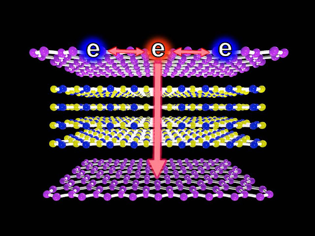
To solve that, the researchers used a completely different approach. They combined single layers of graphene with thin layers of insulating boron nitride to form a sandwich structure, known as a van der Waals heterostructure, which gives electrons two paths to choose from when cooling begins. Either the electrons stay in graphene and cool by bouncing off one another, or they get sucked out of graphene and move through the surrounding layer.

By tuning standard experimental knobs, such as voltage and optical pulse energy, the researchers found they can precisely control where the electrons travel and how long they take to cool off. The work provides new ways of seeing electrons cool off at extremely short time scales, and demonstrates novel devices for nanoscale optoelectronics.

This structure is one of the first in a new class of devices that are synthesized by mechanically stacking atomically thin membranes. By carefully choosing the materials that make up the device, the researchers developed a new type of optoelectronic photodetector that is only 10 nanometers thick. Such devices address the technological drive for ultra-dense, low-power, and ultra-efficient devices for integrated circuits.

The research follows advances made in 2011 Science article, in which the research team discovered the fundamental importance of hot electrons in the optoelectronic response of devices based on graphene.

Other co-authors of the Nature Physics paper are: Qiong Ma, Trond I. Andersen, Nityan L. Nair, Andrea F. Young, Wenjing Fang, Jing Kong, Nuh Gedik and Pablo Jarillo-Herrero, all of the Massachusetts Institute of Technology; Mathieu Massicotte and Frank H. L. Koppens, both of The Institute of Photonic Sciences in Spain; and Kenji Watanabe and Takashi Taniguchi, both of the National Institute for Materials Science in Japan.


Tuesday, November 10, 2015

New Technology Colors In the Infrared Rainbow


Traditional infrared imaging systems may look colorful on screen, with warm objects appearing redder and whiter than their surroundings. But these images are not created from actual colors.

They are based on the amount of thermal radiation&mdashor infrared light&mdashthat the camera captures.

The ability to identify different wavelengths&mdashor colors&mdashof the infrared spectrum would capture much more information about the objects being imaged, such as their chemical composition.

In a new study, a team lead by Maiken H. Mikkelsen, the Nortel Networks Assistant Professor of Electrical & Computer Engineering and Physics at Duke University, demonstrates perfect absorbers for small bands of the electromagnetic spectrum from visible light through the near infrared. The fabrication technique is easily scalable, can be applied to any surface geometry and costs much less than current light absorption technologies.

Once adopted, the technique would allow advanced thermal imaging systems to not only be produced faster and cheaper than today’s counterparts, but to have higher sensitivity. It could also be used in a wide variety of other applications, such as masking the heat signatures of objects.

The study was published online Nov. 9 in Advanced Materials.


“By borrowing well-known techniques from chemistry and employing them in new ways, we were able to obtain significantly better resolution than with a million-dollar state-of-the-art electron beam lithography system,” said Mikkelsen. “This allowed us to create a coating that can fine-tune the absorption spectra with a level of control that hasn’t been possible previously, with potential applications from light harvesting and photodetectors to military applications.”

“This doesn’t require top-down fabrication such as expensive lithography techniques and we don’t make this in a clean room,” added Gleb Akselrod, a postdoctoral researcher in Mikkelsen’s laboratory.  “We build it from the bottom up, so the whole thing is inherently cheap and very scalable to large areas.”

The technology relies on a physics phenomenon called plasmonics. The researchers first coat a surface with a thin film of gold through a common process like evaporation. They then put down a few-nanometer-thin layer of polymer, followed by a coating of silver cubes, each one about 100 nanometers (billionths of a meter) in size.

When light strikes the new engineered surface, a specific color gets trapped on the surface of the nanocubes in packets of energy called plasmons, and eventually dissipates into heat. By controlling the thickness of the polymer film and the size and number of silver nanocubes, the coating can be tuned to absorb different wavelengths of light from the visible spectrum to the near infrared. 

“What is so attractive about the film/nanocube system is its remarkable simplicity and flexibility,” said David R. Smith, the James B. Duke Professor of Electrical and Computer Engineering at Duke. “The unique absorbing properties of the nanocubes can be predicted with straightforward formulas, making it easy to quickly determine recipes for surface coatings that provide desired spectral properties. The nanocube system eliminates, or at least vastly reduces, cost and manufacturing issues, so that we can focus on impacting exciting application areas such as photovoltaics or thermal coatings.”

For an example of the latter, if you can control the colors of light that a material absorbs, then you can also control the wavelengths of light that it emits. By making the nanocubes larger to absorb wavelengths corresponding to thermal radiation, this technology could suppress or mask an object’s natural thermal radiation, otherwise known as “black body radiation.”

Coating photodetectors to absorb only specific wavelengths of infrared light would allow novel and cheap cameras to be made that could see different infrared colors.

“We haven’t made the device that’s actually going to take that energy and convert it to an electrical signal yet,” said Akselrod. “That’s going to be the next step.”

This work was supported by the Air Force Office of Scientific Research (FA9550-15-1-0301, FA9550-12-1-0491).

Thursday, September 5, 2013

Engineers make golden breakthrough to improve electronic devices based on molybdenum disulfide

A Kansas State University chemical engineer has discovered that a new member of the ultrathin materials family has great potential to improve electronic and thermal devices.
Vikas Berry, William H. Honstead professor of chemical engineering, and his research team have studied a new three-atom-thick material -- molybdenum disulfide -- and found that manipulating it with gold atoms improves its electrical characteristics. Their research appears in a recent issue of Nano Letters.
The research may advance transistors, photodetectors, sensors and thermally conductive coatings, Berry said. It could also produce ultrafast, ultrathin logic and plasmonics devices.
Berry's laboratory has been leading studies on synthesis and properties of several next-generation atomically thick nanomaterials, such as graphene and boron-nitride layers, which have been applied for sensitive detection, high-rectifying electronics, mechanically strong composites and novel bionanotechnology applications.
"Futuristically, these atomically thick structures have the potential to revolutionize electronics by evolving into devices that will be only a few atoms thick," Berry said.
For the latest research, Berry and his team focused on transistors based on molybdenum disulfide, or MoS2, which was isolated only two years ago. The material is made of three-atom-thick sheets and has recently shown to have transistor-rectification that is better than graphene, which is a single-atom-thick sheet of carbon atoms.
When Berry's team studied molybdenum disulfide's structure, they realized that the sulfur group on its surface had a strong chemistry with noble metals, including gold. By establishing a bond between molybdenum disulfide and gold nanostructures, they found that the bond acted as a highly coupled gate capacitor.
Berry's team enhanced several transistor characteristics of molybdenum disulfide by manipulating it with gold nanomaterials.
"The spontaneous, highly capacitive, lattice-driven and thermally-controlled interfacing of noble metals on metal-dichalcogenide layers can be employed to regulate their carrier concentration, pseudo-mobility, transport-barriers and phonon-transport for future devices," Berry said.
The work may greatly improve future electronics, which will be ultrathin, Berry said. The researchers have developed a way to reduce the power that is required to operate these ultrathin devices.
"The research will pave the way for atomically fusing layered heterostructures to leverage their capacitive interactions for next-generation electronics and photonics," Berry said. "For example, the gold nanoparticles can help launch 2-D plasmons on ultrathin materials, enabling their interference for plasmonic-logic devices."
The research also supports the current work on molybdenum disulfide-graphene-based electron-tunneling transistors by providing a route for direct electrode attachment on a molybdenum disulfide tunneling gate.
"The intimate, highly capacitive interaction of gold on molybdenum disulfide can induce enhanced pseudo-mobility and act as electrodes for heterostructure devices," said T.S. Sreeprasad, a postdoctoral researcher in Berry's group.
The researchers plan to create further complex nanoscale architectures on molybdenum disulfide to build logic devices and sensors.
"The incorporation of gold into molybdenum disulfide provides an avenue for transistors, biochemical sensors, plasmonic devices and catalytic substrate," said Phong Nguyen, a doctoral student in chemical engineering, Wichita, Kan., who is part of Berry's research team.
Namhoon Kim, master's student in grain science and industry, Korea,worked on the research as an undergraduate in chemical engineering.