Wednesday, May 7, 2014

A hydrogel that knows when to go

Brendan Watson with hydrogel
Brendan Watson, a graduate student at Rice University, led a project to create a hydrogel bioscaffold that is liquid at room temperature and instantly solidifies as it approaches body temperature. A second process allows the hydrogel to break down slowly as it is replaced by healthy tissue. Photo by Jeff Fitlow

Rice University bioscaffold material degrades as bone grows to replace it

Rice University bioengineers have created a hydrogel that instantly turns from liquid to semisolid at close to body temperature – and then degrades at precisely the right pace.

The gel shows potential as a bioscaffold to support the regrowth of bone and other three-dimensional tissues in a patient’s body using the patient’s own cells to seed the process.
The hydrogel created in the lab of Rice bioengineer Antonios Mikos is a liquid at room temperature but, when injected into a patient, becomes a gel that would fill and stabilize a space while natural tissue grows to replace it.
The new material detailed in the American Chemical Society journal Biomacromolecules takes the state of the art a few steps further, Rice scientists said.
“This study describes the development of a novel thermogelling hydrogel for stem cell delivery that can be injected into skeletal defects to induce bone regeneration and that can be degraded and eliminated from the body as new bone tissue forms and matures,” said Mikos, Rice’s Louis Calder Professor of Bioengineering and Chemical and Biomolecular Engineering.
Hydrogel turning white
The hydrogel turns from liquid to semisolid as it moves from room temperature to near body temperature in an experiment. The material inside the tube quickly turns white as it gellates. Chemical links in the gel take longer to form, but help it hold its size and shape as a scaffold for growing new tissue. Photo by Jeff Fitlow
A problem with thermogelling polymers is that once they harden, they begin to collapse and then force out water, said Rice graduate student and the paper’s lead author, Brendan Watson. That process, known as syneresis, defeats the purpose of defining the space doctors hope to fill with new tissue.
“If the transition gellation temperature is one or two degrees below body temperature, these polymers slowly start to expel water and shrink down until they’re one-half or one-third the size. Then the defect-filling goal is no longer accomplished,” he said.
Watson and his colleagues at Rice’s BioScience Research Collaborative solved the problem by adding chemical cross-linkers to the gel’s molecules. “It’s a secondary mechanism that, after the initial thermogellation, begins to stabilize the gel,” he said. The links begin to form at the same time as the gel, but crosslinking takes up to a half-hour to complete.
The hydrogel is designed for stability over its long-term use as a scaffold for cells to take root and proliferate. But it’s also designed for its own timely destruction.
“I came up with the idea a few years ago, but it’s finally all come together,” said Watson, who is pursuing both a Rice doctorate and a medical degree in a joint program with nearby Baylor College of Medicine. “These chemical crosslinks are attached by phosphate ester bonds, which can be degraded by catalysts – in particular, alkaline phosphatase – that are naturally produced by bone tissue.
Closeup of gel
What started as a clear liquid at room temperature quickly turns into a white gel at body temperature. Photo by Jeff Fitlow
“The catalysts are naturally present in your body at all times, in low levels. But in areas of newly formed bone, they actually get to much higher levels,” he said. “So what we get is a semismart material for bone-tissue engineering. As new bone is formed, the gel should degrade more quickly in that area to allow even more space for bone to form.”
The fine balancing act took a lot of expertise from his colleagues and co-authors, including Paul Engel, chair of Rice’s Department of Chemistry, and F. Kurtis Kasper, a senior faculty fellow in bioengineering. “It looks like we may have just decided to try something and found that, hey, it worked! But that wasn’t the case,” said Watson, describing the months and years it took to refine the hydrogel. Engel’s help with the sophisticated chemistry was especially valuable, he said.
Watson expects that the material degradation can be tuned to match various bone growth rates.
“Optimizing the degradation kinetics is nontrivial and may be better suited for a biotech company,” he said. “We focus more on the performance of the hydrogels and the underlying molecular mechanisms”
The National Institutes of Health, the Keck Center Nanobiology Training Program of the Gulf Coast Consortia and the Baylor College of Medicine Medical Scientist Training Program supported the research.
http://news.rice.edu/2014/05/07/a-hydrogel-that-knows-when-to-go-2/#sthash.qW7y7eWn.dpuf

Discovery Creates a Better Chance for Clean Energy Research

This is a magnified image of a new thermoelectric 
material discovered by University of Houston researchers.
Credit: University of Houston
UH Researchers Find First New High-Efficiency Thermoelectric Material in 60 Years

University of Houston physicists have discovered a new thermoelectric material offering high performance at temperatures ranging from room temperature up to 300 degrees Celsius, or about 573 degrees Fahrenheit.
“This new material is better than the traditional material, Bismuth telluride, and can be used for waste heat conversion into electricity much more efficiently,” said Zhifeng Ren, M.D. Anderson Chair professor of physics at UH and the lead author of a paper describing the discovery, published online by Nano Energy.
Ren, who is also principal investigator at the Texas Center for Superconductivity at UH, said the work could be important for clean energy research and commercialization at temperatures of about 300 degrees Celsius.
Bismuth telluride has been the standard thermoelectric material since the 1950s and is used primarily for cooling, although it can also be used at temperatures up to 250 C, or 482 F, for power generation, with limited efficiency.
For this discovery, Ren and other members of his lab used a combination of magnesium, silver and antimony to generate electricity from heat using the thermoelectric principle. They added a small amount of nickel, after which Ren said the compound worked even better.
The work was done in collaboration with researchers from the UH Department of Chemistry and the Massachusetts Institute of Technology. Huaizhou Zhao and Jiehe Sui, a member of Ren’s lab whose home institute is the Harbin Institute of Technology in China, were primary contributors; Zhao is now a research scientist at the Institute of Physics with the Chinese Academy of Sciences.
The material works well up to 300 C, Ren said; work to improve its efficiency is ongoing.
The potential for capturing heat – from power plants, industrial smokestacks and even vehicle tailpipes – and converting it into electricity is huge, allowing heat that is currently wasted to be used to generate power. Ren said temperatures there can range from 200 C to 1,000 C, and until now, there hasn’t been a thermoelectric material capable of working once conditions get beyond the lower levels of heat. Much of the demand ranges from 250 C to 300 C, he said.
Ren long has worked in thermoelectrics, among other scientific fields. His research group published an article in the journal Science in 2008 establishing that the efficiency – the technical term is the “figure of merit” – of Bismuth telluride could be increased as much as 20 percent by changing how it is processed. At the time, Ren was at Boston College.  
And his lab last summer published a paper in the Proceedings of the National Academy of Sciences establishing tin telluride with the addition of the chemical element indium as a material capable of converting waste heat to electricity. But tin telluride works best at temperatures higher than about 300 C, or about 573 F, making it important to continue looking for another material that works at lower temperatures.
Ren’s group isn’t the first to study the new material, which has not been named but is referred to in the Nano Energy paper as simply MgAgSb-based materials, using the chemical names for the elements used to create it. The paper cites work done in 2012 by M.J. Kirkham, et al; that work used magnesium, silver and antimony in equal parts, Ren said, but resulted in impurities and poor conducting properties.  
He said his lab found that using slightly less silver and antimony, and mixing the elements separately – putting magnesium and silver first in the ball milling process, adding the antimony after several hours – eliminated the impurities and significantly improved the thermoelectric properties.
“We had much different qualities,” he said. “Better, with no impurities, and smaller grain size, along with much better thermoelectric properties.”
http://www.uh.edu/news-events/stories/2014/May/0507RenThermoelectrics.php

Tuesday, May 6, 2014

New chemistry paves the way for creating higher-quality advanced materials

Imperial scientists have developed a new technique for carrying out multiple-step chemical reactions to improve production of advanced materials.
The technique allows chemists to do multiple-step reactions inside tiny droplets in a flowing stream – a process known as droplet chemistry – and should make it possible to carry out more sophisticated chemical reactions than have previously been possible. The method will make it easier to create high-quality, high-performance advanced materials for new plastic electronics such as flexible computer screens and affordable solar panels. The Imperial researchers describe their new ‘three-phase multistep droplet reactor’ in a paper in the journal Nature Communications.
Droplet chemistry is a form of “flow chemistry” where reactive chemicals combine, mix, and react inside networks of narrow pipes or channels to create new materials. In conventional forms of flow chemistry the reaction solution moves through the pipes as a continuous stream, and over time residue may deposit on the channel walls, causing fouling.
In droplet chemistry, the reaction solution flows as discrete droplets inside a second liquid that it cannot mix with. This prevents channel-fouling as the droplets are kept away from the walls of the reactor by the other liquid. The small size of the droplets also improves the uniformity of the reaction, leading to a better quality product.
One of the lead researchers, Adrian Nightingale, then a postdoctoral researcher in the Department of Chemistry, said: “When arteries become blocked the whole circulatory system can quickly fail, with fatal consequences. Similarly, when the tubes we use in flow chemistry become blocked, flow reactors fail and production stops. Droplet-based chemistry eradicates this problem, but previously it could only be used for very simple, single-step reactions where all reagents were present in the droplets from the outset. Here we have developed a method for controllably injecting new reagents into the flowing droplets, greatly expanding the palette of materials that can be produced.”
In the new research, the scientists have introduced a third phase, a gas, alongside the two liquids to establish an even spacing between the droplets and so ensure that each one receives the same dose of the added reagent.
John de Mello, who heads up the research team, likened the challenge to throwing small parcels into the open windows of passing cars. “If the cars are all moving at the same speed and are exactly the same distance apart, you can time things well and achieve a perfect success rate. That’s what the gas is needed for – to maintain a uniform separation between droplets.”
James Bannock from Imperial’s Doctoral Training Centre In Plastic Electronics commented: “This three-phase droplet chemistry provides an incredibly controlled, straightforward and low cost method for carrying out the multistep chemical procedures needed to create robust and high-quality advanced materials.”
Tom Phillips, also a co-author of the work, added: “This step forward is very exciting for industry as the method should scale well to higher production volumes, allowing high-specification advanced materials to be made in the quantities that industry needs.”
The scientists compared the performance of the three-phase reactor to conventional droplet reactors by using a simple visual test. They added a continuous stream of red dye to a droplet stream of blue dye, and then they recorded images of the droplets before and after the red dye was added. Without the gas, there were irregularities in the spacing between the droplets after dye was added and significant variations in their size and colouration due to inconsistent dosing. With the gas present, all droplets were uniformly spaced and had the same purple colour after dye was added, indicating that each droplet had received the exact same dose of dye.
The scientists used their new three-phase chemical reactor to create quantum dots, which are nanocrystals made of semiconductors most commonly used in solar cells and medical imaging. They believe the technique will be readily applicable to a broad range of fine chemicals and advanced materials.
Source: http://www3.imperial.ac.uk/newsandeventspggrp/imperialcollege/newssummary/news_6-5-2014-10-46-17

Friday, May 2, 2014

High Quality Three-Dimensional Nanoporous Graphene

Nanoporous graphene on nanoporous Ni (left) and Nanoporous graphene after dissolving the nanoporous Ni substrate.


Three-dimentional (3D) nanoporous graphene with preserved 2D Dirac electronic characters was successfully synthesized by Dr. Yoshikazu Ito and Prof. Mingwei CHEN at Advanced Institute for Materials Research (AIMR), Tohoku University. The nanoporous graphene is constructed by a single layer graphene sheet that is continuously inter-connected to form a complex 3D network structure. This free-standing nanoporous graphene with an excellent crystallinity possesses high mobility, holding great promise for the applications in electronic devices.

The nanoporous graphene were grown by a nanoporous metal based chemical vapor deposition (CVD) method as shown in Figure 1(a). The overall morphology of the nanoporous graphene in Figure 1(b) shows a ~20 µm thick free-standing bulk sheet. Although the 3D nanoporous graphene has a complex structure, it is demonstrated to be 500 cm2/Vs in electron mobility and a mass-less Dirac cone system. As the conventional transistor requires electron mobility of 200 cm2/Vs, it is greatly expected that this nanoporous graphene will bring a new device which can be replaced with Si devices.
This work is collaborated with the research teams of Prof. Katsumi Tanigaki and Prof. Takashi Takahashi at AIMR, Tohoku University. This research results will be published in issue 19 of 'Angewandte Chemie International Edition' as a Hot Paper on 2 May.

Introduction
Graphene is a mono-layer carbon material with low cost, high chemical/thermal stability, and ultrahigh strength and is expected to be a replacement of silicon and noble metals for electron devices, battery materials, photo-/ion detectors and catalysts. Although some of graphene products such as display and electrodes are commercially available, the applications are limited due to the 2D sheet structure. In other words, the performance per gram is excellent but the performance per volume cannot be achieved easily. Therefore, many efforts have been made to construct the 2D material as a 3D structure with retained physical/chemical properties and high volumetric performance. However, the reported 3D nanoporous carbon materials suffer from poor mobility because of the lower crystallinity, which cannot be used for the electron devices. To achieve semiconductor-grade 3D carbon materials, the monolayer graphene sheet with a high crystalline structure is required in a 3D structure. Thus, we have developed a 3D nanoporous graphene with preserved high mobility and unique 2D electronic properties of graphene.

Research content
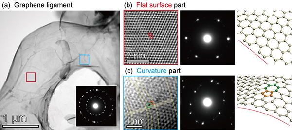
The nanoporous graphene in Figure 1 were synthesized by the nanoporous metal based CVD method. The nanoporous graphene fully inherits the geometric structure of the nanoporous nickel substrate after dissolving nickel. The atomic structure of the nanoporous graphene was observed by TEM as shown in Figure 2. The ligament in Figure 2(a) were constructed by flat surface parts (Figure 2(b)) and curvature parts (Figure 2(c)) of the graphene sheet. It is obvious that the six-membered rings were observed in the flat part while the five- and seven-membered rings were observed in the curved parts due to the geometrical requirement to create the curvature structures.
pr_140407_02.jpgFigure 2. Morphology of 3D nanoporous graphene. (a) 3D ligament structures, (b) flat part and (c) curvature part on the graphene sheet with atomic models, respectively.
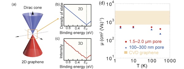
The physical properties of the nanoporous graphene were investigated. As the 2D graphene is a Dirac cone system (Figure 3(a)) and shows a linear dispersion electronic density of state (Figure 3(b)). The 3D nanoporous graphene in Figure 2 also demonstrates a linear relationship near the Fermi level, which is similar with the 2D graphene. The electron mobility of the nanoporous graphene with different pore sizes was measured. As the temperature increase, the electron mobility slightly decreases to 200-400 cm2/Vs. As compared with 2D CVD graphene, the electron mobility is still high enough for device applications.
pr_140407e_04.jpgFigure 3. (a) Dirac cone dispersion of 2 D graphene. (b) Typical 2D graphene electronic density of state. (c) Electronic density of state of 3D nanoporous graphene (experiment) (d) Temperature and porous size dependence of electron mobility. Orange area shows the electron mobility range of CVD graphene. The electron mobility of silicon is 1500 cm2/Vs.
In conclusion, the nanoporous graphene preserves 2D graphene futures. These findings are firstly reported for revealing the physical properties of 3D nanoporous graphene.

Future visions
The 3D nanoporous graphene is expected to bring breakthrough of solving a problem of volumetric performance of 2D graphene by providing abundant porous structures for an easy mass transport and large effective surface area. Moreover, the nanoporous graphene preserves 2D graphene electronic characters and expected to be employed for applications in electronic devices such as a transistors and condensers.

http://www.wpi-aimr.tohoku.ac.jp/en/news/press/2014/20140407_000460.html

Thursday, May 1, 2014

Playing Pool with Carbon Atoms

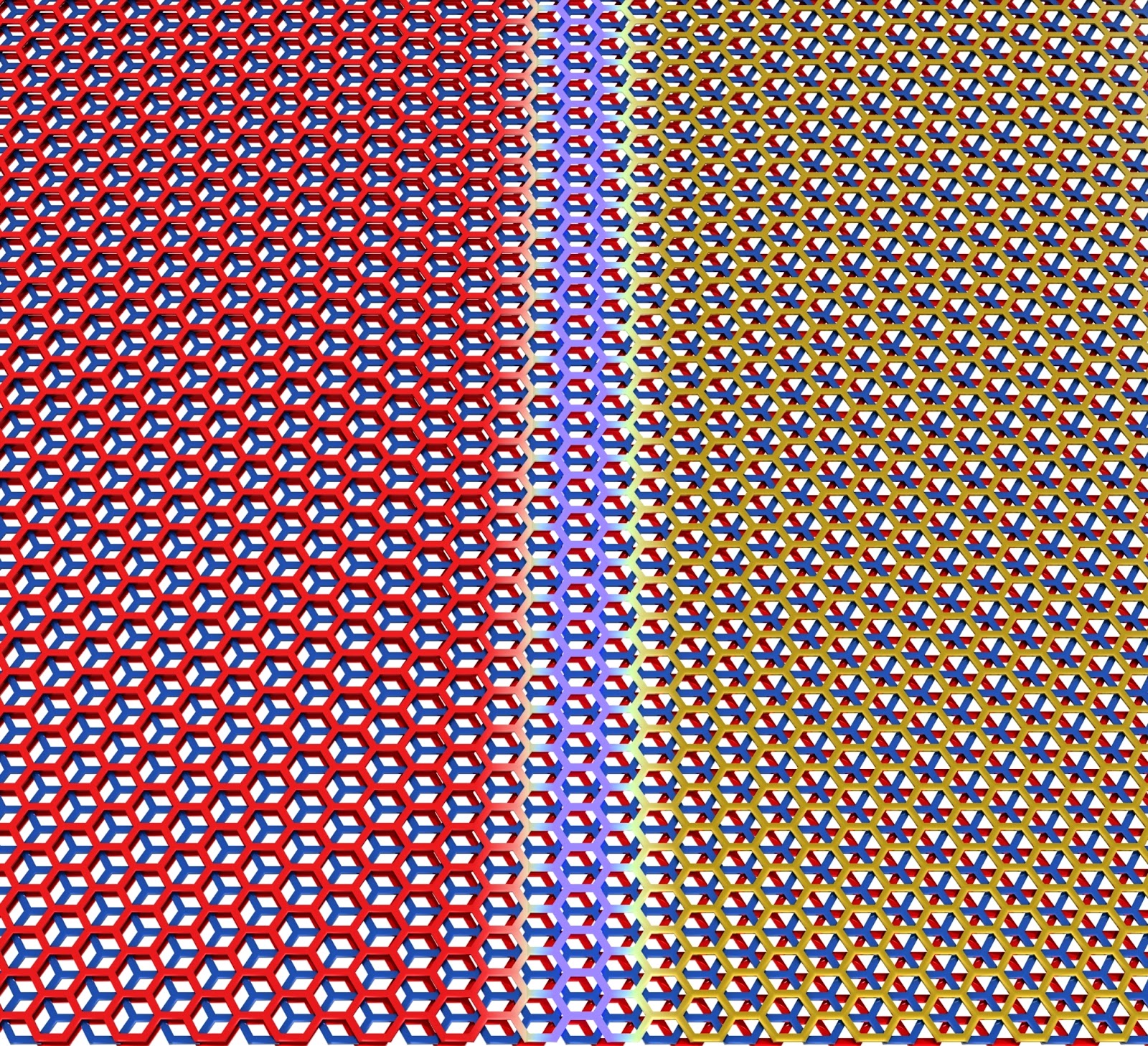
Graphene trilayers can be stacked in two
different configurations, which can occur naturally
in the same flake. They are separated by
a sharp boundary. (Image: Pablo San-Jose ICMM-CSI)
A University of Arizona-led team of physicists has discovered how to change the crystal structure of graphene, more commonly known as pencil lead, with an electric field, an important step toward the possible use of graphene in microprocessors that would be smaller and faster than current, silicon-based technology. 
Graphene consists of extremely thin sheets of graphite: when writing with a pencil, graphene sheets slough off the pencil's graphite core and stick to the page. If placed under a high-powered electron microscope, graphene reveals its sheet-like structure of cross-linked carbon atoms, resembling chicken wire.
When manipulated by an electric field, parts of the material are transformed from behaving as a metal to behaving as a semiconductor, the UA physicists found.
Graphene is the world’s thinnest material, with 300,000 sheets needed to amount to the thickness of a human hair or a sheet of paper. Scientists and engineers are interested in it because of its possible applications in microelectronic devices, in hopes of propelling us from the silicon age to the graphene age. The tricky part is to control the flow of electrons through the material, a necessary prerequisite for putting it to work in any type of electronic circuit.
Brian LeRoy, UA associate professor of physics, and his collaborators have cleared a hurdle toward that goal by showing that an electric field is capable of controlling the crystal structure of trilayer graphene – which is made up of three layers of graphene.
Most materials require high temperatures, pressure or both to change their crystal structure, which is the reason why graphite doesn't spontaneously turn into diamond or vice versa. 
"It is extremely rare for a material to change its crystal structure just by applying an electric field," LeRoy said. "Making trilayer graphene is an exceptionally unique system that could be utilized to create novel devices."
Trilayer graphene can be stacked in two unique ways. This is analogous to stacking layers of billiards balls in a triangular lattice, with the balls representing the carbon atoms.
"When you stack two layers of billiards balls, their 'crystal structure' is fixed because the top layer of balls must sit in holes formed by the triangles of the bottom layer," explained Matthew Yankowitz, a third-year doctoral student in LeRoy's lab in the Department of Physics in the UA College of Science. He is the first author on the published research, which appears in the journal Nature Materials. "The third layer of balls may be stacked in such a way that its balls are flush above the balls in the bottom layer, or it may be offset slightly so its balls come to lie above the holes formed by triangles in the bottom layer."
These two stacking configurations can naturally exist in the same flake of graphene. The two domains are separated by a sharp boundary where the carbon hexagons are strained to accommodate the transition from one stacking pattern to the other.
"Due to the different stacking configurations on either side of the domain wall, one side of the material behaves as a metal, while the other side behaves as a semiconductor," LeRoy explained.
While probing the domain wall with an electric field, applied by an extremely sharp metal scanning tunneling microscopy tip, the researchers in LeRoy's group discovered that they could move the position of the domain wall within the flake of graphene. And as they moved the domain wall, the crystal structure of the trilayer graphene changed in its wake. 
"We had the idea that there would be interesting electronic effects at the boundary, and the boundary kept moving around on us," LeRoy said. "At first it was frustrating, but once we realized what was going on, it turned out to be the most interesting effect." 
By applying an electric field to move the boundary, it is now possible for the first time to change the crystal structure of graphene in a controlled fashion.
"Now we have a knob that we can turn to change the material from metallic into semiconducting and vice versa to control the flow of electrons," LeRoy said. "It basically gives us an on-off switch, which had not been realized yet in graphene."
While more research is needed before graphene can be applied in technological applications on an industrial scale, researchers see ways it may be used.
"If you used a wide electrode instead of a pointed tip, you could move the boundary between the two configurations a farther distance, which could make it possible to create transistors from graphene,” Yankowitz said.
Transistors are a staple of electronic circuits because they control the flow of electrons.
Unlike silicon transistors used now, graphene-based transistors could be extremely thin, making the device much smaller, and since electrons move through graphene much faster than through silicon, the devices would enable faster computing.
In addition, silicon-based transistors are being manufactured to function as one of two types – p-type or n-type – whereas graphene could operate as both. This would make them cheaper to produce and more versatile in their applications.
The other contributors to the research paper, "Electric field control of soliton motion and stacking in trilayer graphene," include Joel I-Jan Wang (Massachusetts Institute of Technology and Harvard University in Cambridge, Massachusetts), A. Glen Birdwell (U.S. Army Research Laboratory, Adelphi, Maryland), Yu-An Chen (MIT), K. Watanabe and T. Taniguchi (National Institute for Materials Science, Tsukuba, Japan), Philippe Jacquod (UA Department of Physics), Pablo San-Jose (Instituto de Ciencia de Materiales de Madrid) and Pablo Jarillo-Herrero (MIT).
The study appears in the advance online publication of Nature Materials.

http://uanews.org/story/playing-pool-with-carbon-atoms