Showing posts with label graphite. Show all posts

Tuesday, October 13, 2015

Discovery about new battery overturns decades of false assumptions


Abundant potassium than rarer lithium used

New findings at Oregon State University have overturned a scientific dogma that stood for decades, by showing that potassium can work with graphite in a potassium-ion battery - a discovery that could pose a challenge and sustainable alternative to the widely-used lithium-ion battery.

Lithium-ion batteries are ubiquitous in devices all over the world, ranging from cell phones to laptop computers and electric cars. But there may soon be a new type of battery based on materials that are far more abundant and less costly. A potassium-ion battery has been shown to be possible. And the last time this possibility was explored was 1932.

"For decades, people have assumed that potassium couldn't work with graphite or other bulk carbon anodes in a battery," said Xiulei (David) Ji, the lead author of the study and an assistant professor of chemistry in the College of Science at Oregon State University.

"That assumption is incorrect," Ji said. "It's really shocking that no one ever reported on this issue for 83 years."

The Journal of the American Chemical Society published the findings from this discovery, which was supported by the U.S. Department of Energy and done in collaboration with OSU researchers Zelang Jian and Wei Luo. A patent is also pending on the new technology.

The findings are of considerable importance, researchers say, because they open some new alternatives to batteries that can work with well-established and inexpensive graphite as the anode, or high-energy reservoir of electrons. Lithium can do that, as the charge carrier whose ions migrate into the graphite and create an electrical current.

Aside from its ability to work well with a carbon anode, however, lithium is quite rare, found in only 0.0017 percent, by weight, of the Earth's crust. Because of that it's comparatively expensive, and it's difficult to recycle. Researchers have yet to duplicate its performance with less costly and more readily available materials, such as sodium, magnesium, or potassium.

"The cost-related problems with lithium are sufficient that you won't really gain much with economies of scale," Ji said. "With most products, as you make more of them, the cost goes down. With lithium the reverse may be true in the near future. So we have to find alternatives."

That alternative, he said, may be potassium, which is 880 times more abundant in the Earth's crust than lithium. The new findings show that it can work effectively with graphite or soft carbon in the anode of an electrochemical battery. Right now, batteries based on this approach don't have performance that equals those of lithium-ion batteries, but improvements in technology should narrow the gap, he said.

"It's safe to say that the energy density of a potassium-ion battery may never exceed that of lithium-ion batteries," he said. "But they may provide a long cycling life, a high power density, a lot lower cost, and be ready to take the advantage of the existing manufacturing processes of carbon anode materials."

Electrical energy storage in batteries is essential not only for consumer products such as cell phones and computers, but also in transportation, industry power backup, micro-grid storage, and for the wider use of renewable energy.

OSU officials say they are seeking support for further research and to help commercialize the new technology, through the OSU Office of Commercialization and Corporate Development.

Thursday, May 1, 2014

Playing Pool with Carbon Atoms

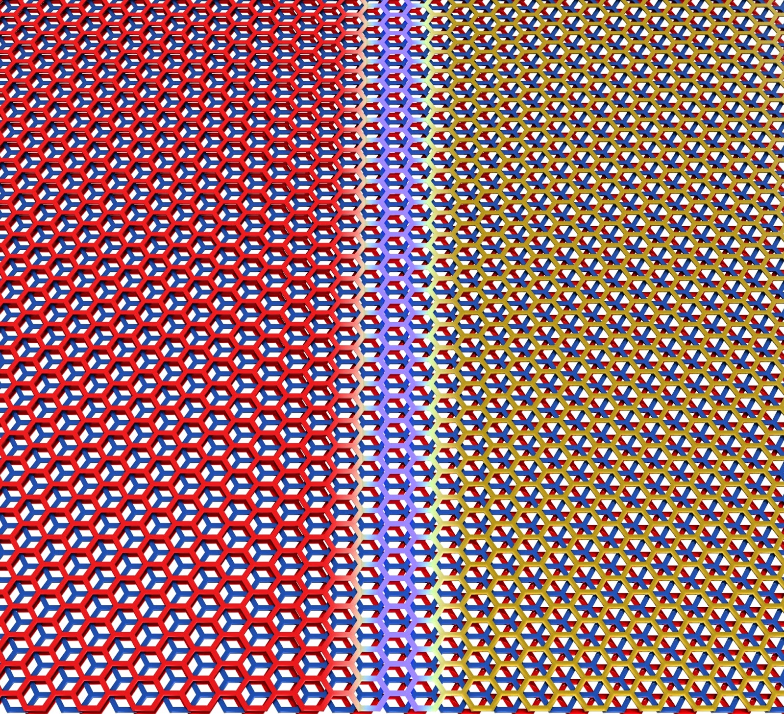
Graphene trilayers can be stacked in two
different configurations, which can occur naturally
in the same flake. They are separated by
a sharp boundary. (Image: Pablo San-Jose ICMM-CSI)
A University of Arizona-led team of physicists has discovered how to change the crystal structure of graphene, more commonly known as pencil lead, with an electric field, an important step toward the possible use of graphene in microprocessors that would be smaller and faster than current, silicon-based technology. 
Graphene consists of extremely thin sheets of graphite: when writing with a pencil, graphene sheets slough off the pencil's graphite core and stick to the page. If placed under a high-powered electron microscope, graphene reveals its sheet-like structure of cross-linked carbon atoms, resembling chicken wire.
When manipulated by an electric field, parts of the material are transformed from behaving as a metal to behaving as a semiconductor, the UA physicists found.
Graphene is the world’s thinnest material, with 300,000 sheets needed to amount to the thickness of a human hair or a sheet of paper. Scientists and engineers are interested in it because of its possible applications in microelectronic devices, in hopes of propelling us from the silicon age to the graphene age. The tricky part is to control the flow of electrons through the material, a necessary prerequisite for putting it to work in any type of electronic circuit.
Brian LeRoy, UA associate professor of physics, and his collaborators have cleared a hurdle toward that goal by showing that an electric field is capable of controlling the crystal structure of trilayer graphene – which is made up of three layers of graphene.
Most materials require high temperatures, pressure or both to change their crystal structure, which is the reason why graphite doesn't spontaneously turn into diamond or vice versa. 
"It is extremely rare for a material to change its crystal structure just by applying an electric field," LeRoy said. "Making trilayer graphene is an exceptionally unique system that could be utilized to create novel devices."
Trilayer graphene can be stacked in two unique ways. This is analogous to stacking layers of billiards balls in a triangular lattice, with the balls representing the carbon atoms.
"When you stack two layers of billiards balls, their 'crystal structure' is fixed because the top layer of balls must sit in holes formed by the triangles of the bottom layer," explained Matthew Yankowitz, a third-year doctoral student in LeRoy's lab in the Department of Physics in the UA College of Science. He is the first author on the published research, which appears in the journal Nature Materials. "The third layer of balls may be stacked in such a way that its balls are flush above the balls in the bottom layer, or it may be offset slightly so its balls come to lie above the holes formed by triangles in the bottom layer."
These two stacking configurations can naturally exist in the same flake of graphene. The two domains are separated by a sharp boundary where the carbon hexagons are strained to accommodate the transition from one stacking pattern to the other.
"Due to the different stacking configurations on either side of the domain wall, one side of the material behaves as a metal, while the other side behaves as a semiconductor," LeRoy explained.
While probing the domain wall with an electric field, applied by an extremely sharp metal scanning tunneling microscopy tip, the researchers in LeRoy's group discovered that they could move the position of the domain wall within the flake of graphene. And as they moved the domain wall, the crystal structure of the trilayer graphene changed in its wake. 
"We had the idea that there would be interesting electronic effects at the boundary, and the boundary kept moving around on us," LeRoy said. "At first it was frustrating, but once we realized what was going on, it turned out to be the most interesting effect." 
By applying an electric field to move the boundary, it is now possible for the first time to change the crystal structure of graphene in a controlled fashion.
"Now we have a knob that we can turn to change the material from metallic into semiconducting and vice versa to control the flow of electrons," LeRoy said. "It basically gives us an on-off switch, which had not been realized yet in graphene."
While more research is needed before graphene can be applied in technological applications on an industrial scale, researchers see ways it may be used.
"If you used a wide electrode instead of a pointed tip, you could move the boundary between the two configurations a farther distance, which could make it possible to create transistors from graphene,” Yankowitz said.
Transistors are a staple of electronic circuits because they control the flow of electrons.
Unlike silicon transistors used now, graphene-based transistors could be extremely thin, making the device much smaller, and since electrons move through graphene much faster than through silicon, the devices would enable faster computing.
In addition, silicon-based transistors are being manufactured to function as one of two types – p-type or n-type – whereas graphene could operate as both. This would make them cheaper to produce and more versatile in their applications.
The other contributors to the research paper, "Electric field control of soliton motion and stacking in trilayer graphene," include Joel I-Jan Wang (Massachusetts Institute of Technology and Harvard University in Cambridge, Massachusetts), A. Glen Birdwell (U.S. Army Research Laboratory, Adelphi, Maryland), Yu-An Chen (MIT), K. Watanabe and T. Taniguchi (National Institute for Materials Science, Tsukuba, Japan), Philippe Jacquod (UA Department of Physics), Pablo San-Jose (Instituto de Ciencia de Materiales de Madrid) and Pablo Jarillo-Herrero (MIT).
The study appears in the advance online publication of Nature Materials.

http://uanews.org/story/playing-pool-with-carbon-atoms

Wednesday, August 28, 2013

A nano-graphite cold cathode for an energy-efficient cathodoluminescent light source

Abstract

The development of new types of light sources is necessary in order to meet the growing demands of consumers and to ensure an efficient use of energy. The cathodoluminescence process is still under-exploited for light generation because of the lack of cathodes suitable for the energy-efficient production of electron beams and appropriate phosphor materials. In this paper we propose a nano-graphite film material as a highly efficient cold cathode, which is able to produce high intensity electron beams without energy consumption. The nano-graphite film material was produced by using chemical vapor deposition techniques. Prototypes of cathodoluminescent lamp devices with a construction optimized for the usage of nano-graphite cold cathodes were developed, manufactured and tested. The results indicate prospective advantages of this type of lamp and the possibility to provide advanced power efficiency as well as enhanced spectral and other characteristics.
Keywords: cathodoluminescence; electron field emission; light source; nano-graphite; vacuum electronics
Top

Introduction

The fundamental importance of light in our lives cannot be overstated. The sun is the only natural source of light emission with appropriate intensity. This is the driving force for the elaboration of artificial light sources. The demand on artificial lighting increases constantly and will continue to increase in the future. The conversion of electric energy is the most practical way for light generation and it is currently used in incandescent bulbs, gas discharge, and electroluminescent lamps of various designs, shapes, input and output power. Additionally, a photoluminescent process is used to convert blue or ultraviolet radiation, produced by gas discharge or by electroluminescence, to white light. Unfortunately, because of the fundamental principles of nature, the energy efficient generation of light requires the usage of extremely toxic materials (mercury, heavy metals and others). This leads to the necessity of expensive and laborious efforts to dispose of the mercury-based fluorescent devices and the semiconductor-based light emitting diode (LED) lamps (see, e.g., [1,2]). Moreover, the spectral characteristics of the light produced by these fluorescent and LED lamps are often not perceived as pleasing in contrast to incandescent lamps. But incandescent bulbs convert only 5% of the consumed energy into light and are thus considered as ineffective. The other 95% of the energy are transformed into heat, which cannot be considered as waste in many countries where electricity is used for house heating practically every day. In the “energy efficient” fluorescent and LED lamps the energy conversion ratio is about 10%, so that there is a decrease of energy loss on heating only from 95 to 90%. At the same time, production costs for these lamps, i.e. consumption and waste of energy at the production plant, are many times higher compared to the production costs of incandescent bulbs.
Thus, the development of new types of light sources is necessary to provide better energy efficiency, spectral characteristics, and other properties desired by the consumer. The process of cathodoluminescence (CL), which is potentially able to provide a conversion of up to 35% [3] (or more for nanostructured phosphors [4]) of the energy of the excited electron into radiation, is therefore attractive for light generation [5]. The most suitable source of electrons is the field emission (FE) cathode [5], allowing to exploit the FE effect for the creation of CL light emitting lamps. Cathodes of this type (also called "cold cathodes") are capable of generating intense electron beams virtually without any energy consumption because of the quantum tunneling nature of the FE effect [6]. Individual field emitters are required to have a needle- or blade-shape with a high aspect ratio in order to provide a sufficient intensity of the electric field at moderate voltages. Multi-emitter cathodes are necessary to achieve a reasonable total intensity of electron beams, because the current from a single emitter is limited due to its small emission surface area. To prevent field shielding the individual emitters, composing flat multi-emitter FE cathodes, must be separated from each other by a distance a few times larger than the height of the emitters [7,8]. To survive under the action of the extremely strong electric field, FE cathodes must be made from rather strong materials – hard metals, or selected semiconductors. From this point of view graphite-like materials, having the strongest interatomic interaction, are attractive for the FE cathode production. In this paper we describe the production technique and the electron field emission (FE) characteristics of nano-graphite films (NGF) and prototypes of CL lamps with NGF cold cathodes.

Results and Discussion: http://www.beilstein-journals.org/bjnano/single/articleFullText.htm?publicId=2190-4286-4-58


Tuesday, August 20, 2013

3D Graphene: Solar Power's Next Platinum?

One of the most promising types of solar cells has a few drawbacks. A scientist at Michigan Technological University may have overcome one of them.
Dye-sensitized solar cells are thin, flexible, easy to make and very good at turning sunshine into electricity. However, a key ingredient is one of the most expensive metals on the planet: platinum. While only small amounts are needed, at $1,500 an ounce, the cost of the silvery metal is still significant.
Yun Hang Hu, the Charles and Caroll McArthur Professor of Materials Science and Engineering, has developed a new, inexpensive material that could replace the platinum in solar cells without degrading their efficiency: 3D graphene.
Regular graphene is a famously two-dimensional form of carbon just a molecule or so thick. Hu and his team invented a novel approach to synthesize a unique 3D version with a honeycomb-like structure. To do so, they combined lithium oxide with carbon monoxide in a chemical reaction that forms lithium carbonate (Li2CO3) and the honeycomb graphene. The Li2CO3 helps shape the graphene sheets and isolates them from each other, preventing the formation of garden-variety graphite.  Furthermore, the Li2CO3 particles can be easily removed from 3D honeycomb-structured graphene by an acid.
The researchers determined that the 3D honeycomb graphene had excellent conductivity and high catalytic activity, raising the possibility that it could be used for energy storage and conversion. So they replaced the platinum counter electrode in a dye-sensitized solar cell with one made of the 3D honeycomb graphene. Then they put the solar cell in the sunshine and measured its output.
The cell with the 3D graphene counter electrode converted 7.8 percent of the sun’s energy into electricity, nearly as much as the conventional solar cell using costly platinum (8 percent).
Synthesizing the 3D honeycomb graphene is neither expensive nor difficult, said Hu, and making it into a counter electrode posed no special challenges.
The research has been funded by the American Chemical Society Petroleum Research Fund (PRF-51799-ND10) and the National Science Foundation (NSF-CBET-0931587). The article describing the work, “3D Honeycomb-Like Structured Graphene and Its High Efficiency as a Counter-Electrode Catalyst for Dye-Sensitized Solar Cells,” coauthored by Hu, Michigan Tech graduate student Hui Wang, Franklin Tao of the University of Notre Dame, Dario J. Stacchiola of Brookhaven National Laboratory and Kai Sun of the University of Michigan, was published online July 29 in the journal Angewandte Chemie, International Edition.
Michigan Technological University (www.mtu.edu) is a leading public research university developing new technologies and preparing students to create the future for a prosperous and sustainable world. Michigan Tech offers more than 130 undergraduate and graduate degree programs in engineering; forest resources; computing; technology; business; economics; natural, physical and environmental sciences; arts; humanities; and social sciences