 |
| Nanoporous graphene on nanoporous Ni (left) and Nanoporous graphene after dissolving the nanoporous Ni substrate. |
Three-dimentional (3D) nanoporous graphene with preserved 2D Dirac electronic characters was successfully synthesized by Dr. Yoshikazu Ito and Prof. Mingwei CHEN at Advanced Institute for Materials Research (AIMR), Tohoku University. The nanoporous graphene is constructed by a single layer graphene sheet that is continuously inter-connected to form a complex 3D network structure. This free-standing nanoporous graphene with an excellent crystallinity possesses high mobility, holding great promise for the applications in electronic devices.
The nanoporous graphene were grown by a nanoporous metal based chemical vapor deposition (CVD) method as shown in Figure 1(a). The overall morphology of the nanoporous graphene in Figure 1(b) shows a ~20 µm thick free-standing bulk sheet. Although the 3D nanoporous graphene has a complex structure, it is demonstrated to be 500 cm2/Vs in electron mobility and a mass-less Dirac cone system. As the conventional transistor requires electron mobility of 200 cm2/Vs, it is greatly expected that this nanoporous graphene will bring a new device which can be replaced with Si devices.
This work is collaborated with the research teams of Prof. Katsumi Tanigaki and Prof. Takashi Takahashi at AIMR, Tohoku University. This research results will be published in issue 19 of 'Angewandte Chemie International Edition' as a Hot Paper on 2 May.
Introduction
Graphene is a mono-layer carbon material with low cost, high chemical/thermal stability, and ultrahigh strength and is expected to be a replacement of silicon and noble metals for electron devices, battery materials, photo-/ion detectors and catalysts. Although some of graphene products such as display and electrodes are commercially available, the applications are limited due to the 2D sheet structure. In other words, the performance per gram is excellent but the performance per volume cannot be achieved easily. Therefore, many efforts have been made to construct the 2D material as a 3D structure with retained physical/chemical properties and high volumetric performance. However, the reported 3D nanoporous carbon materials suffer from poor mobility because of the lower crystallinity, which cannot be used for the electron devices. To achieve semiconductor-grade 3D carbon materials, the monolayer graphene sheet with a high crystalline structure is required in a 3D structure. Thus, we have developed a 3D nanoporous graphene with preserved high mobility and unique 2D electronic properties of graphene.
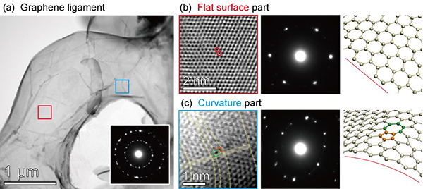
The nanoporous graphene in Figure 1 were synthesized by the nanoporous metal based CVD method. The nanoporous graphene fully inherits the geometric structure of the nanoporous nickel substrate after dissolving nickel. The atomic structure of the nanoporous graphene was observed by TEM as shown in Figure 2. The ligament in Figure 2(a) were constructed by flat surface parts (Figure 2(b)) and curvature parts (Figure 2(c)) of the graphene sheet. It is obvious that the six-membered rings were observed in the flat part while the five- and seven-membered rings were observed in the curved parts due to the geometrical requirement to create the curvature structures.
 Figure 2. Morphology of 3D nanoporous graphene. (a) 3D ligament structures, (b) flat part and (c) curvature part on the graphene sheet with atomic models, respectively.
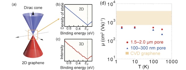
The physical properties of the nanoporous graphene were investigated. As the 2D graphene is a Dirac cone system (Figure 3(a)) and shows a linear dispersion electronic density of state (Figure 3(b)). The 3D nanoporous graphene in Figure 2 also demonstrates a linear relationship near the Fermi level, which is similar with the 2D graphene. The electron mobility of the nanoporous graphene with different pore sizes was measured. As the temperature increase, the electron mobility slightly decreases to 200-400 cm2/Vs. As compared with 2D CVD graphene, the electron mobility is still high enough for device applications.
 Figure 3. (a) Dirac cone dispersion of 2 D graphene. (b) Typical 2D graphene electronic density of state. (c) Electronic density of state of 3D nanoporous graphene (experiment) (d) Temperature and porous size dependence of electron mobility. Orange area shows the electron mobility range of CVD graphene. The electron mobility of silicon is 1500 cm2/Vs.
In conclusion, the nanoporous graphene preserves 2D graphene futures. These findings are firstly reported for revealing the physical properties of 3D nanoporous graphene.
The 3D nanoporous graphene is expected to bring breakthrough of solving a problem of volumetric performance of 2D graphene by providing abundant porous structures for an easy mass transport and large effective surface area. Moreover, the nanoporous graphene preserves 2D graphene electronic characters and expected to be employed for applications in electronic devices such as a transistors and condensers.
http://www.wpi-aimr.tohoku.ac.jp/en/news/press/2014/20140407_000460.html

No comments:
Post a Comment