Monday, November 25, 2013

Decay used to construct quantum information


An artists impression of the experiment. Four ions are trapped on a line. The outer Magnesium ions (green) cools the system by emitting light. Lasers are used to prepare the inner Beryllium ions (red) in an entangled state where one can not understand the state of the particles individually but have to consider the two ions as a whole. As opposed to previous experiments also the latter process happens by the emission of light. (Credit NIST).
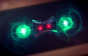
Usually, when researchers work with quantum information, they do everything they can to prevent the information from decaying. Now researchers at the Niels Bohr Institute, among others, have flipped things around and are exploiting the decay to create the so-called entanglement of atomic systems, which is the foundation for quantum information processing. The results are published in the scientific journal, Nature.
“When working with quantum information, you would normally seek to isolate the system from the environment in order to not get a disturbing interaction that can destroy the fragile quantum state. But this is very difficult to avoid completely. So we thought that you could perhaps take the opposite approach and instead of seeing decay as the enemy, look at it as a friend and take advantage of it,” explains Anders Søndberg Sørensen, a professor of quantum optics at the Niels Bohr Institute at the University of Copenhagen. 

Electrons leaping hither and thither

The problem is that the quantum system is affected by the environment and exchanges energy with it. The electrons in the atoms jump from one energy state to another and researchers consider this kind of jump to be decay, because the information stored in the electrons disappears into its surroundings.  
“But with our method we let the quantum system ‘talk’ with its surroundings and create a control of the electrons’ jumps so that they are precisely in the state we want them to be in, and in that way we make use of the interaction with the environment,” explains PhD student Florentin Reiter, who developed the theoretical model for the method together with Anders Sørensen.
The ion trap used in the experiment. Electrical potential are applied through thin gold wires on a chip and used to trap ions in a narrow slot. (Credit NIST).
The research is a collaboration with the experimental research group lead by David Wineland (recipient of the Nobel Prize in physics last year) at the National Institute for Standards and Technology in Boulder Colorado, USA.

Kicking the electrons into place

The method is based on a chain of ions comprised of magnesium and beryllium. They are cooled down to near absolute zero at minus 273 degrees C. The magnesium atoms are just there as a kind of cooling element in the chain of ions, while the beryllium atoms are the active elements. Entanglement is created between the electrons of the beryllium ions using carefully controlled laser light.
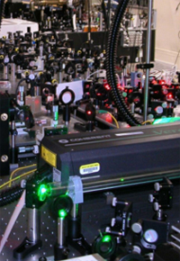
The lab where the experiment was performed. (Credit NIST).
“The trick lies in the combination of laser light,” explains Florentin Reiter and continues “the electrons can be in four energy states and if they jump around and land in a ‘wrong’ state, they are simply ‘kicked’ by the laser and we continue until they are where they are supposed to be. In that way there is perfect entanglement. Unlike in the past, when you had to use carefully designed laser pulses to create entanglement, researchers can now just turn on the laser and grab a cup of coffee and when they come back the electrons are in the correct state.”
Up until this point, the decay of quantum information has been the biggest obstacle to making a quantum computer. The new experiment is the first time the problem has been turned on its head and the decay has been used constructively in a quantum computer. The researchers hope that this might be a way to overcome some of the problems that have previously made it difficult to make quantum computers. The researchers are now working to make more advanced quantum information processors based on the same ideas. In particular, they hope that similar techniques can be used to correct errors in a quantum computer. 

Friday, November 22, 2013

Milestone could help magnets end era of computer transistors

As current passes through a strip of tantalum, electrons
with opposite spins separate. Researchers used the resulting
polarization to create a nanomagnetic switch that
could one day replace computer transistors.
(Image by Debanjan Bhowmik, UC Berkeley)
New work by researchers at UC Berkeley could soon transform the building blocks of modern electronics by making nanomagnetic switches a viable replacement for the conventional transistors found in all computers.

Semiconductor-based transistors, the on-off switches that direct the flow of electricity and form a computer’s nervous system, have been consuming greater chunks of power at increasingly hotter temperatures as processing speeds grow. For more than a decade, researchers have been pursuing magnets as an alternative to transistors because they require far less energy needs when switching. However, until now, the power needed to generate the magnetic field to orient the magnets so they can easily clock on and off has negated much of the energy savings that would have been gained by moving away from transistors.
UC Berkeley researchers overcame this limitation by exploiting the special properties of the rare, heavy metal tantalum.
In a paper published online Sunday, Nov. 17, in the journal Nature Nanotechnology, the researchers describe how they created a so-called Spin Hall effect by using nanomagnets placed on top of tantalum wire and then sending a current through the metal. Electrons in the current will randomly spin in either a clockwise or counterclockwise direction. When the current is sent through tantalum’s atomic core, the metal’s physical properties naturally sort the electrons to opposing sides based on their direction of spin. This creates the polarization researchers exploited to switch magnets in a logic circuit without the need for a magnetic field.
“This is a breakthrough in the push for low-powered computing,” said study principal investigator Sayeef Salahuddin, UC Berkeley assistant professor of electrical engineering and computer sciences. “The power consumption we are seeing is up to 10,000 times lower than state-of-the-art schemes for nanomagnetic computing. Our experiments are the proof of concept that magnets could one day be a realistic replacement for transistors.”
Other co-authors of the study are graduate student and lead author Debanjan Bhowmik, and Long You, a research scholar.
The Defense Advanced Research Projects Agency, Semiconductor Research Corp. and the National Science Foundation helped support this work.

Will 2-D Tin be the Next Super Material?

Stanene Lattice
Adding fluorine atoms (yellow) to a single layer of tin atoms (grey) 
should allow a predicted new material, stanene, to conduct 
electricity perfectly along its edges (blue and red arrows) at  
temperatures up to 100 degrees Celsius (212 Fahrenheit). 
(Yong Xu/Tsinghua University; Greg Stewart/SLAC)


Theorists Predict New Single-Layer Material Could Go Beyond Graphene, Conducting Electricity with 100 Percent Efficiency at Room Temperature
A single layer of tin atoms could be the world’s first material to conduct electricity with 100 percent efficiency at the temperatures that computer chips operate, according to a team of theoretical physicists led by researchers from the U.S. Department of Energy’s (DOE) SLAC National Accelerator Laboratory and Stanford University.
Researchers call the new material "stanene," combining the Latin name for tin (stannum) with the suffix used in graphene, another single-layer material whose novel electrical properties hold promise for a wide range of applications.
"Stanene could increase the speed and lower the power needs of future generations of computer chips, if our prediction is confirmed by experiments that are underway in several laboratories around the world," said the team leader, Shoucheng Zhang, a physics professor at Stanford and the Stanford Institute for Materials and Energy Sciences (SIMES), a joint institute with SLAC. The team’s work was published recently in Physical Review Letters.
The Path to Stanene
For the past decade, Zhang and colleagues have been calculating and predicting the electronic properties of a special class of materials known as topological insulators, which conduct electricity only on their outside edges or surfaces and not through their interiors. When topological insulators are just one atom thick, their edges conduct electricity with 100 percent efficiency. These unusual properties result from complex interactions between the electrons and nuclei of heavy atoms in the materials.
“The magic of topological insulators is that by their very nature, they force electrons to move in defined lanes without any speed limit, like the German autobahn,” Zhang said. “As long as they’re on the freeway – the edges or surfaces – the electrons will travel without resistance.”
In 2006 and 2009, Zhang’s group predicted that mercury telluride and several combinations of bismuth, antimony, selenium and tellurium should be topological insulators, and they were soon proven right in experiments performed by others. But none of those materials is a perfect conductor of electricity at room temperature, limiting their potential for commercial applications.
Earlier this year, visiting scientist Yong Xu, who is now at Tsinghua University in Beijing, collaborated with Zhang’s group to consider the properties of a single layer of pure tin.
“We knew we should be looking at elements in the lower-right portion of the periodic table,” Xu said. “All previous topological insulators have involved the heavy and electron-rich elements located there.”
Their calculations indicated that a single layer of tin would be a topological insulator at and above room temperature, and that adding fluorine atoms to the tin would extend its operating range to at least 100 degrees Celsius (212 degrees Fahrenheit).
Ultimately a Substitute for Silicon?
Zhang said the first application for this stanene-fluorine combination could be in wiring that connects the many sections of a microprocessor, allowing electrons to flow as freely as cars on a highway. Traffic congestion would still occur at on- and off-ramps made of conventional conductors, he said. But stanene wiring should significantly reduce the power consumption and heat production of microprocessors.
Manufacturing challenges include ensuring that only a single layer of tin is deposited and keeping that single layer intact during high-temperature chip-making processes.
“Eventually, we can imagine stanene being used for many more circuit structures, including replacing silicon in the hearts of transistors,” Zhang said. “Someday we might even call this area Tin Valley rather than Silicon Valley.”
Additional contributors included researchers from Tsinghua University in Beijing and the Max Planck Institute for Chemical Physics of Solids in Dresden, Germany. The research was supported by the Mesodynamic Architectures program of the Defense Advanced Research Projects Agency.
SLAC is a multi-program laboratory exploring frontier questions in photon science, astrophysics, particle physics and accelerator research. Located in Menlo Park, California, SLAC is operated by Stanford University for the U.S. Department of Energy Office of Science. To learn more, please visitwww.slac.stanford.edu.
The Stanford Institute for Materials and Energy Sciences (SIMES) is a joint institute of SLAC National Accelerator Laboratory and Stanford University. SIMES studies the nature, properties and synthesis of complex and novel materials in the effort to create clean, renewable energy technologies. For more information, please visit simes.slac.stanford.edu.
DOE’s Office of Science is the single largest supporter of basic research in the physical sciences in the United States, and is working to address some of the most pressing challenges of our time. For more information, please visit science.energy.gov.

Thursday, November 21, 2013

Before Cells, Biochemicals May Have Combined in Clay

Clay – an assortment of silicates leached from
rock by weathering, is made up of tiny disks a
few nanometers (billionths of a meter) across,
as seen in an electron microscope photo, above.
The disks have negative charges on the flat
surface and positive charges around the rim.
Herded by charged ions in sea water the disks
join in a “house of cards” structure that makes
 a spongy mass.
Clay – a seemingly infertile blend of minerals – might have been the birthplace of life on Earth. Or at least of the complex biochemicals that make life possible, Cornell University biological engineers report in the Nov. 7 online issue of the journal Scientific Reports, published by Nature Publishing.
“We propose that [in early geological history] clay hydrogel provided a confinement function for biomolecules and biochemical reactions,” said Dan Luo, professor of biological and environmental engineering and a member of the Kavli Institute at Cornell for Nanoscale Science.
In simulated ancient seawater, clay forms a hydrogel – a mass of microscopic spaces capable of soaking up liquids like a sponge. Over billions of years, Luo explained, chemicals confined in those spaces could have carried out the complex reactions that formed proteins, DNA and eventually all the machinery that makes a living cell work. Clay hydrogels could have confined and protected those chemical processes until the membrane that surrounds living cells developed, he said.

The Luo group previously has used synthetic hydrogels as a “cell-free” medium for protein production. Fill the spongy material with DNA, amino acids, the right enzymes and a few bits of cellular machinery and you can make the proteins for which the DNA encodes, just as you might in a vat of cells. To make the process useful for producing large quantities of proteins, such as for drug manufacturing, you need a lot of hydrogel, so the researchers set out to find a cheaper way to make it. Postdoctoral researcher Dayong Yang noticed that clay formed a hydrogel. Why consider clay? “It’s dirt cheap,” said Luo. Better yet, it turned out unexpectedly that using clay enhanced protein production.
But then it occurred to the researchers that what they had discovered might answer a long-standing question about how biomolecules evolved. Experiments by the late Carl Sagan of Cornell and others have shown that amino acids and other biomolecules could have been formed in primordial oceans, drawing energy from lightning or volcanic vents. But in the vast ocean, how could these molecules come together often enough to assemble into more complex structures, and what protected them from the harsh environment? Scientists previously suggested that tiny balloons of fat or polymers might have served as precursors of cell membranes. Clay is a promising possibility because biomolecules tend to attach to its surface, and theorists have shown that cytoplasm – the interior environment of a cell – behaves much like a hydrogel. And, Luo said, a clay hydrogel better protects its contents from damaging enzymes (called “nucleases”) that might dismantle DNA and other biomolecules.
As further evidence, geological history shows that clay first appeared – as silicates leached from rocks – just at the time biomolecules began to form into protocells – cell-like structures, but incomplete – and eventually membrane-enclosed cells. The geological events matched nicely with biological events.
How these biological machines evolved remains to be explained, Luo said. For now his research group is working to understand why a clay hydrogel works so well, with an eye to practical applications in cell-free protein production.
Luo collaborated with Max Lu, a professor at the Australian Institute for Bioengineering and Nanotechnology at the University of Queensland in Australia. The work was performed at the Cornell Center for Materials Research Shared Facilities, supported by the National Science Foundation.


Nanoparticles Could Improve Chemical Sensors


Scanning electron microscope images of SnO2 “nano-flowers” synthesized for gas sensor researchIMAGE COURTESY OF MARK ANDIO
Patricia Morris, associate professor of materials science and engineering, leads a team of researchers who have developed new methods for making materials for gas sensors that could be used to detect toxic industrial chemicals and biological warfare agents.
The goal is to design a material with long-term stability that responds quickly and accurately to a variety of chemicals at very low concentrations. These sensor devices are similar to the human nose, which coordinates signals from hundreds of thousands of sensory neurons to identify gases. Similarly, the artificial sensor uses a combination of electrical responses from sensor arrays to identify the concentration of a specific gas.

The group’s efforts include synthesizing metal-oxide particles in the form of nanoparticles, nano-structured materials and hollow particles for use as the sensing material to increase sensor performance. NiO and SnO2nanoparticles, for example, are created with a particle size between five and 10 nanometers. Five nanometers (billionths of a meter) is approximately 50 atoms in diameter.“These are sensors that a soldier could wear on the battlefield, or a first responder could wear to an accident at a chemical plant,” Morris says.
In order to make the particles, precursors are placed in a Teflon-lined pressure vessel that is heated in an oven. The combination of temperature and pressure involving the correct precursors leads to the formation of nanoparticles in such a way that they have large surface areas to capture molecules from the air, enabling the sensor to detect very small quantities of a substance.
For instance, the SnO2nano-structured particles, sometimes referred to as “nanoflowers” due to their appearance, have many surfaces advantageous for adsorption and detection of hazardous gases. These materials have shown fast response and recovery times — meaning quicker detection — compared to other metal-oxide materials used for sensors.
Once the metal-oxide materials are synthesized, the particles are suspended in liquids designed to have the proper viscosity and surface tension in order to deposit the materials controllably on sensor platforms. Morris and her colleagues use a sophisticated inkjet printer that dispenses picoliter-volume drops onto very small microsensor substrates consisting of a silicon chip fitted with a platinum heater and gold electrodes to monitor the material’s electrical resistance. The change in the material’s resistance corresponds to a change in the surrounding atmosphere.
“Each material is sensitive to specific gases, and both oxides can be used in an array to selectively detect a gas in a complex background,” says Mark Andio, a materials science and engineering doctoral student working with Morris on the nano-structured oxides research.
Now that the researchers know the various chemical steps that take place during the synthesis of the materials, they can devise ways to add chemical dopants to the nanoparticles to change the function of the sensor — for instance, to speed up the response rate.