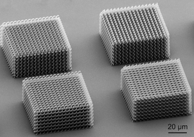
Shown below is a series of structures fabricated by means of the direct laser writing process achieved with Photonic Professional systems.
 |
| 3D square spiral structure out of SU-8. |
 |
| Three-dimensional photonic crystal of cubic symmetry fabricated by two photon polymerization. |
 |
| Three-dimensional photonic crystal of cubic symmetry fabricated by two photon polymerization. |
 |
| Bi-chiral photonic crystals, produced by the group of Prof. Dr. Martin Wegener (KIT) |
 |
| 3D photonic quasicrystal with a five-fold rotational symmetry. The structure was written into the photoresist SU-8. Image: Dr. Alexandra Ledermann (KIT) |
 |
| Circular spirals seen from above. This structure was written into the chalcogenide glass As2S3. |
 |
| Further examples of 3D structures consisting of circular spirals. |
 |
| 3D photonic crystal structure according to the layout provided by Mr. Ivan Shishkin, ITMO, Russia. |
 |
| 3D photonic crystal known under the acronym SP2 - standing for slanted pore structure. Originally proposed for anisotropic etching techniques or GLAD "2" stands for the number of separate drilling/etching/GLAD-processes. With our technique these structure can directly be written into a photosensitive material in one step. Later on these structures can be replicated or inverted e.g. in silicon with our techniques. |


No comments:
Post a Comment