Showing posts with label electron. Show all posts

Wednesday, January 20, 2016

Watching Electrons Cool in 30 Quadrillionths of a Second


Two University of California, Riverside assistant professors of physics are among a team of researchers that have developed a new way of seeing electrons cool off in an extremely short time period.

The development could have applications in numerous places where heat management is important, including visual displays, next-generation solar cells and photodetectors for optical communications.

In visual displays, such as those used in cell phones and computer monitors, and photodetectors, which have a wide variety of applications including solar energy harvesting and fiber optic telecommunications, much of the energy of the electrons is wasted by heating the material.

Controlling the flow of heat in the electrons, rather than wasting this energy by heating the material, could potentially increase the efficiency of such devices by converting excess energy into useful power.

The research is outlined in a paper, “Tuning ultrafast electron thermalization pathways in a van der Waals heterostructure,” published online Monday (Jan. 18) in the journal Nature Physics. Nathan Gabor and Joshua C.H. Lui, assistant professors of physics at UC Riverside, are among the co-authors.

In electronic materials, such as those used in semiconductors, electrons can be rapidly heated by pulses of light.  The time it takes for electrons to cool each other off is extremely short, typically less than 1 trillionth of a second.

To understand this behavior, researchers use highly specialized tools that utilize ultra-fast laser techniques. In the two-dimensional material graphene cooling excited electrons occurs even faster, taking only 30 quadrillionths of a second. Previous studies struggled to capture this remarkably fast behavior.


To solve that, the researchers used a completely different approach. They combined single layers of graphene with thin layers of insulating boron nitride to form a sandwich structure, known as a van der Waals heterostructure, which gives electrons two paths to choose from when cooling begins. Either the electrons stay in graphene and cool by bouncing off one another, or they get sucked out of graphene and move through the surrounding layer.

By tuning standard experimental knobs, such as voltage and optical pulse energy, the researchers found they can precisely control where the electrons travel and how long they take to cool off. The work provides new ways of seeing electrons cool off at extremely short time scales, and demonstrates novel devices for nanoscale optoelectronics.

This structure is one of the first in a new class of devices that are synthesized by mechanically stacking atomically thin membranes. By carefully choosing the materials that make up the device, the researchers developed a new type of optoelectronic photodetector that is only 10 nanometers thick. Such devices address the technological drive for ultra-dense, low-power, and ultra-efficient devices for integrated circuits.

The research follows advances made in 2011 Science article, in which the research team discovered the fundamental importance of hot electrons in the optoelectronic response of devices based on graphene.

Other co-authors of the Nature Physics paper are: Qiong Ma, Trond I. Andersen, Nityan L. Nair, Andrea F. Young, Wenjing Fang, Jing Kong, Nuh Gedik and Pablo Jarillo-Herrero, all of the Massachusetts Institute of Technology; Mathieu Massicotte and Frank H. L. Koppens, both of The Institute of Photonic Sciences in Spain; and Kenji Watanabe and Takashi Taniguchi, both of the National Institute for Materials Science in Japan.


Sunday, November 15, 2015

Superconductor survives ultra-high magnetic field


Physicists from the universities of Groningen and Nijmegen (the Netherlands) and Hong Kong have discovered that transistors made of ultrathin layers molybdeendisulfide (MoS2) are not only superconducting at low temperatures but also stay superconducting in a high magnetic field. This is a unique phenomenon with exciting promises for the future. The experiments were the first to have been performed at the High Field Magnet Laboratory in Nijmegen, jointly operated by Radboud University and the FOM foundation. The results are published on 12 November by the journal Science.

Superconductivity is a state in which the electrical resistance of a material disappears completely. Normally, this phenomenon only exists at low temperatures and disappears under a high magnetic field. But in the High Field Magnet Laboratory (HFML), physicists discovered that MoS2 -- which can be bought at the home depot stores as dry lubricant -- remains superconducting under a high magnetic field of 37.5 Tesla.

Strongly pinned electron pairs Superconductivity is induced when free electrons in a material are attracted to each other and form weakly bonded electron pairs. These pairs condensate to a superconducting state only when all possible disturbances in the material are minimal and therefore, superconductivity usually exists at very low temperature. When a material is exposed to a magnetic field, the weak bonding between the electron pair can be easily broken. The rupture of the pair destroys the superconductivity when disturbance from the magnetic field becomes strong enough.

Surprisingly, the superconducting state of MoS2 survives high magnetic fields because the paired electrons are intrinsically associated with an internal high magnetic field, which can reach nearly one hundred Tesla, much higher than the 37.5 Tesla provided by the HFML. For comparison: a conventional fridge magnet has a magnetic field of approximately 0.1 Tesla. Uli Zeitler, physicist at the HFML at Radboud University explains: 'MoS2 behaves in a way that contradicts a law in physics, the so called Pauli paramagnetic limit.'

Information in electron spin Although the current publication is very fundamental, Zeitler does have some ideas for future applications. 'There is information stored inside the charge and spin of electrons, the direction of their internal magnetic field. If you can influence this spin, for instance with an electric field, you can store information in there. And in principle, this technique could be used in the development of a future quantum computer.'

The described experiments are complicated to perform. 'We execute this research at very low temperatures between 0 and 12 Kelvin, about minus 270 degrees Celsius, and under high magnetic fields. But in order to pump enough electrons into MoS2, we first needed relatively high temperatures of about minus 50 degrees Celsius', Zeitler explains.

As the first external user of the newly-built 37.5 T magnet, Justin Ye, a physicist from Zernike Institute of Advanced Material at the University of Groningen is really excited by the result: 'It is a good starting point of this new facility. As the first user I am very happy to obtain this important result with the support from my colleagues in HFML. Following this breakthrough in identifying a new paring mechanism with stunning protection of superconductivity against high magnetic field, I would expect a lot of unexpected results from the future experiments in HFML.'

Monday, September 14, 2015

First realization of an electric circuit with a magnetic insulator using spin waves


Physicists at the University of Groningen, together with colleagues from Utrecht and Brest, have discovered a new principle governing how information is sent between electronic circuits. This could also help generate electricity more efficiently from temperature differences. The results were published on 14 September in the journal Nature Physics.

The research was led by Bart van Wees, Professor of Applied Physics at the University of Groningen and specialist in fields such as spintronics. This is a form of electronics in which not only the electrons count, but their spin is important too. Each electron has a spin, a quantum mechanical phenomenon that can have two values: up or down. You can ‘code’ an electron with information and transport it using ‘spin currents’.

In the new research Ludo Cornelissen, a PhD student supervised by Van Wees, showed that spin currents could pass through isolators too. In the experiment a conductive material was combined with a non-conductive magnetic material. When electrons collide with the non-conductive material they cannot continue, but a change in the magnetization occurs during the collision that means that the spin is passed on.


‘We designed an experiment where we converted an electron current into a spin wave. It then turned back into an electron current a bit further along,’ Van Wees explains. The spin wave in the non-conductive magnetic material is what is known as a magnon, a disruption in the magnetization that spreads like a wave does through a full stadium: electrons in the material pass the spin on to their neighbours before falling back into their original position. With this form of transport only the spin moves, and the electrons do not travel around. This means heat does not develop and the transport requires very little energy.

‘We are therefore the first to have linked the concept of spin transport to magnetization dynamics and to have shown that spin transport is also possible in isolators’, explains Van Wees. That presents new possibilities. ‘During the transport through the isolator you can manipulate the spin wave, for example through magnetic fields’, explains Van Wees. Spin waves gradually die down due to interaction with the atoms in the crystal grid, but Van Wees and his colleagues have shown that the spin wa0-+ve is maintained for at least 10 micrometres. ‘And that is plenty long enough.

However, the longer the wave, the more sensitive it is to change. You could, for example, use it to make sensors that detect magnetism.’

It is also possible to use a spin wave to switch magnetic bits. ‘With spin waves you can switch a smaller surface than with electromagnetic techniques, and the energy consumption is much better too.’ Such applications are not necessarily that far away. ‘I prefer to work with normal materials at room temperature so that the step to applications is small.’

Another possible application is in thermoelectricity, the conversion of temperature differences into electricity. ‘Materials that are suited to this are all electrical conductors, but an electrical conductor will by definition also conduct heat. This means that part of the temperature difference will leak away.’ The few companies that want to bring thermoelectricity onto the market are therefore struggling with yields that are way below the theoretical possibilities. ‘With our material you can generate a spin current in an isolator that therefore does not let any heat through. That opens the way to a higher yield.’

Thursday, March 27, 2014

Controlling electron spins by light


The picture shows the characteristic
spin texture (arrows) in a topological
insulator (bottom) and how it is
either probed by circularly polarized
light (top) or manipulated by it (middle).
Picture: Rader/Sachez-Barriga/HZB
Researchers of HZB manipulate the electron spin at the surface of topological insulators systematically by light
Topological insulators are considered a very promising material class for the development of future electronic devices. A research team at Helmholtz-Zentrum Berlin (HZB) has discovered, how light can be used to alter the physical properties of the electrons in these materials. Their results have just been published by the renowned journal "Physical Review X".
The material class of topological insulators has been discovered a few years ago and displays amazing properties: In their inside, they behave electrically insulating but at their surface they form metallic, conducting states. The electron spin, i. e., their intrinsic angular momentum, is playing a decisive role. Their sense of rotation is directly coupled to their direction of movement. This coupling leads not only to a high stability of the metallic property but also enables a particularly lossless electrical conduction. Topological insulators are, therefore, considered interesting and promising candidates for novel devices in information technology.

A particularly innovative approach is to try and influence the electron spin at the surface in such devices by light. HZB researcher Prof. Oliver Rader and his team have discovered by which means the spin at the surface of topological insulators can be altered. To this end, the researches performed experiments with light of various energies or wavelengths.
The wavelenght counts
At the synchrotron radiation source BESSY II they investigated the topological insulator bismuth selenide (Bi2Se3) using a method called "spin-resolved photoelectron spectroscopy" – and gained astonishing insights: They found an astonishing difference depending on whether the electrons at the surface of the material are excited with circularly polarized light in the vacuum ultraviolet (50-70 electron volts, eV) or in the ultraviolet spectral range (6 eV). They could demonstrate that they can measure the spin of the electrons without changing it at higher energies which are typically used at synchtrotron light sources. "When excited at 50 eV, the emitted electros display the typical spin texture of topological insulators", Dr. Jaime Sánchez-Barriga, who conducted the experiments, explains. "The electron spins are in the surface aligned on a circle, similarly to a traffic sign for roundabout." This is the ground state of the electrons in the surface of topological insulators."
When excited by low-energy circularly polarized photons (6 eV), the spin of the electrons moved completely out of the surface plane. Above all, they adopted the spin orientation imposed by the right- or left-circularly polarized light. This means that the spin can be systematically manipulated – depending on the light that is used. The scientists can also explain the entirely different behavior at different energies which they attribute to symmetry properties. "Our result delivers important insight how lossless currents could be induced in topological insulators", Oliver Rader explains. "This is important for the development of so-called optospintronic devices which could enormously enhance the speed at which information is stored and processed."
Source: http://www.helmholtz-berlin.de/pubbin/news_seite?nid=13952&sprache=en&typoid=49880

Thursday, January 30, 2014

Scientists discover long-awaited synthetic particle


Researchers have now created and photographed synthetic magnetic monopoles under laboratory conditions. These observations lay the foundation for the underlying structure of the natural magnetic monopole – the detection of which would be a revolutionary event comparable to the discovery of the electron. The results were recently published in Nature magazine.
Although predicted over 80 years ago, the fundamentally quantum-mechanical configuration of the monopoles has not previously been observed in any physical system. The reported results demonstrate the structure in an ultracold atomic gas.
“Our achievement opens up amazing avenues for quantum research. It feels incredible to have been a part of such a major breakthrough,” says a delighted Dr. Mikko Möttönen from Aalto University, Finland.
Evidence for magnetic monopoles has been sought in sources as diverse as lunar samples and ancient micas. The multibillion-euro LHC particle accelerator at CERN has also been used in the search – but no magnetic monopoles have been convincingly identified. The discovery of the synthetic monopole provides a stronger foundation for these efforts.
“The creation of a synthetic magnetic monopole should provide us with unprecedented insight into aspects of the natural monopole,” says Prof. David S. Hall from Amherst College, USA. “It's not every day that you get to poke and prod the analogue of an elusive fundamental particle under highly controlled conditions in the laboratory.”, he continues.
“Synthesis of the monopole is the starting point for many new breakthroughs in quantum physics research. In the future, we want to get even a more complete correspondence with the natural magnetic monopole.”, says Dr. Möttönen.
A magnetic monopole is a particle just like an electron, but with a magnetic rather than an electric charge. Some 80 years ago Paul A. M. Dirac, one of the founders of quantum physics, discovered a quantum-mechanical structure allowing the existence of magnetic monopoles. Dirac’s original framework has now been experimentally realized for the first time.
Figure caption. Artistic illustration of the synthetic magnetic monopole (Heikka Valja)


Further information

Mikko_Mottonen.jpgMikko Möttönen, docent, Dr. Tech.
Aalto University
Department of Applied Physics and O. V. Lounasmaa Laboratory
QCD Labs
mikko.mottonen*at*aalto.fi
tel. +358 50 594 0950
http://physics.aalto.fi/qcd//
Mikko Möttönen is the leader of the theoretical and computational part of the research. Theoretical ideas and computational modelling was very important for the success of the creation of the monopole. The modelling was carried out using the supercomputers at CSC — IT Center for Science Ltd.

David_S_Hall.jpg
David S. Hall, Professor
Amherst College
Department of Physics
dshall@amherst.edu
tel. +1 413 542 2072
http://www3.amherst.edu/~halllab/
David S. Hall is the leader of the experimental part of the research. The synthetic magnetic monopoles were created in the Physics Laboratories at Amherst College, United States of America.


Funding

This material is based upon work supported by the National Science Foundation,Academy of Finland through its Centres of Excellence Program Computational Nanoscience, and Finnish Doctoral Programme in Computational Sciences.


Background information

Magnetic monopole
“A magnetic monopole is an isolated magnetic pole, magnetic charge, and a point-like source of magnetic field.”
An electron is a point-like particle that carries a so-called elementary electric charge. This means that an electron is an isolated source of an electric field.
Can a magnetic field have a similar point-like source?
Every one of us has likely held two bar magnets and noticed that their ends either attract or repel one another. The ends of the magnet are referred to as poles and every magnet has one end that is a north pole and one that is a south pole. A magnetic north pole attracts a magnetic south pole, but repels another north pole. In general, opposite poles attract, and identical poles repel. In this respect, magnetism is very much like electricity, which exhibits the same attractive and repulsive behavior involving positive and negative electric charges.
When a bar magnet breaks, two smaller bar magnets are created, each with its own north and south pole. You can break each of these smaller magnets in two, and so on, and every resulting magnet has a north pole and a south pole. Even at the atomic level, north and south poles always appear together. One cannot produce in this way a solitary pole, or monopole, that acts as a single point source of the magnetic field.
Are there other ways to find magnetic monopoles?
As yet, not a single natural magnetic monopole has been verifiably observed. This was initially considered to be a problem, because theoretical models that described the post-Big-Bang period predicted that they should be quite common. However, a special model for the expansion of the universe was developed that can explain the extreme rarity of these particles.
According to some theories, the energy content (mass) of a single magnetic monopole is so large that if it were completely used to recharge the battery of an electric car, this vehicle would be able to travel for kilometres with the energy. This explains why magnetic monopoles are probably not likely to occur in a particle accelerator. If the mass of a magnetic monopole really is that large, the energy released from the collision of a negatively and positively charged monopole would be as much as the energy released in the explosion of a kilogram of dynamite!
Dirac monopole
“A Dirac monopole is a point-like source of a possibly artificial magnetic field that forms at the endpoint of a quantum whirlpool.”
In quantum mechanics, an electron is described by a diffuse wave-like object rather than a point-like particle. Paul Dirac was the first person to understand the importance of studying the end points of quantum-mechanical whirlpools within these electron waves. He noticed that when an electron has such a terminating vortex, a magnetic monopole inevitably forms at the end point. A terminating vortex is the defining characteristic of the Dirac monopole.
Dirac also noticed that if the universe contains even a single magnetic monopole, it specifies the smallest possible value for an electric charge. All observed charges must be integer multiples of this minimum value; in other words, charge must be quantized. The existence of a monopole would therefore explain the experimental observation that electric charge is quantized.
Dirac monopoles are generally analyzed in a fairly simple quantum-mechanical model. Magnetic monopoles have since been studied in more general, so-called unified field theories, in which they could exist in the absence of a terminating vortex.
Synthetic magnetic field
“A synthetic magnetic field is an artificial field that leads to particle dynamics equivalent to those of an electric charge in a corresponding natural magnetic field.”
Electrons are not the only physical systems that can exhibit terminating vortices. Thus a Dirac monopole can also appear in other systems, such as the Bose-Einstein condensate. Rather than being related to the natural magnetic field, this monopole can be associated with a synthetic magnetic field. Importantly, the structure of the monopole is identical to that of a Dirac magnetic monopole. This is why the Dirac monopole observed in the synthetic magnetic field is closer to a natural magnetic monopole than any earlier observation.
Spin
“Roughly speaking, spin indicates how fast a particle is spinning around its own axis, and the orientation of that axis.”
Spin is a magnetic property of many particles, including electrons, protons, neutrons, and even many types of atoms. For example, the electron spin is composed of two basis states: up or down. This describes whether the electron is spinning around its axis in a clockwise or counter-clockwise direction.
A particle with a non-zero spin creates a magnetic field around it. However, this is not a monopole field – it is a so-called dipole field with both north and south magnetic poles, just like a bar magnet. Even this smallest of bar magnets cannot be broken into two separate magnetic monopoles.
In fact, bar magnets are composed of countless numbers of small spin dipoles, nearly all of which point in the same direction. Overlapping poles of different sign cancel out the field of each other, and thus the field of an ideal bar magnet looks as if it has magnetic poles only at its ends.
Spins tend to align along an externally applied magnetic field, which is the key to the creation of the synthetic magnetic monopole.
Synthesis of a monopole
“A monopole is created in a Bose–Einstein condensate by using an external magnetic field to guide the spins of the atoms forming the condensate.”
In 2009, Aalto University researchers Ville Pietilä and Mikko Möttönen published theoretical results demonstrating a method to create Dirac monopoles in a Bose–Einstein condensate. The idea involves using external magnetic fields to rotate the atomic spins. A Dirac monopole forms in the condensate as a result of the spin rotation. This method was adopted by the researchers in creating the synthetic magnetic monopole.
The Dirac monopole forms in the artificial magnetic field of the condensate, not in the physical magnetic field which steers the spin degree of freedom. Thus, a natural magnetic monopole is not needed to create the synthetic monopole.
 syntetisointi_HQ-pdfliite.jpg
Caption: Synthesis of a monopole in time, starting from panel and ending with panel c. The arrows show the direction of the physical magnetic field produced in the laboratory. This magnetic field also directs the internal spin degree of freedom of the Bose–Einstein condensate in the direction of the arrows. The end result is that the condensate begins to move as if it were electrically charged and affected by a magnetic monopole in the position marked by the black circle in the image. Click for the full-resolution image.
The Bose–Einstein condensate
“A Bose–Einstein condensate behaves like a single giant atom, even though it can contain millions.”
A Bose–Einstein condensate is sometimes considered to be the fifth state of matter, in addition to solid, liquid, gas, and plasma. In the condensate, the importance and location of individual atoms becomes vague and the system behaves as if it were a single large atom. The first Bose–Einstein condensates were achieved in 1995, and this work received the Nobel Prize in 2001.
“Bose–Einstein condensates provide a window from our world into the quantum wonderland. The more often I peek at it, the more I want to stay there,” says enchanted Dr. Möttönen.
Since Bose–Einstein condensates contain many atoms, photographs of them can be taken using technology that is in part similar to that used in ordinary digital cameras. In addition, the condensates can be forced into the desired shape by means of external magnetic fields and laser beams. These properties make condensates a unique tool for developing new phenomena and quantum technologies. In addition to being used with magnetic monopoles, condensates can simulate the properties of various useful materials to the accuracy of a single atom. One of the daydreams of condensate researchers involves finding a solution for the development of superconducting materials that function at room temperature.
What in the world is quantum physics?
“Quantum physics describes natural phenomena most accurately.”
Quantum physics (also quantum mechanics) is a theory developed over the past 100 years that has been observed to describe the reality in more detail than any other model. It is particularly useful for explaining atomic-level phenomena, which is impossible using classical physics. On the other hand, quantum physics reproduces the same results as classical physics on the large scale.
In quantum mechanics, an electron can take on wave-like properties, sometimes appearing as an extended object rather than a point particle. It is this property of extension, which is shared with Bose-Einstein condensates, that permits the observation of the quantum whirlpools essential to detecting the effect of the magnetic monopole.
Quantum technologies use the laws of quantum physics relieved from classical restrictions to produce practical applications. For example, development of a quantum computer – a potentially super-fast problem solver – is one of the key goals of quantum technologies. A quantum computer would be able to find a solution to certain problems very quickly by using methods that are impossible in the logical framework of a normal computer.
“The laws of quantum physics make it possible to take shortcuts. Among other things, this is the basis of the super-fast speed of a quantum computer,” explains Möttönen.
Future directions
In the future, the research groups will concentrate on more in-depth research into the structure of a synthetic magnetic monopole. They are also interested in the dynamics of monopoles and their interactions with other synthetic particles. One interesting idea involves trying to create a monopole that is not bound to a whirlpool in the same way as is the Dirac monopole. This type of structure could possibly describe a natural magnetic monopole in even more detail.
Source: http://sci.aalto.fi/en/current/news/view/2014-01-29/

Tuesday, November 12, 2013

X-rays reveal nano-sized electron sponge

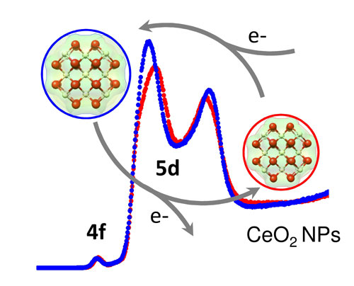
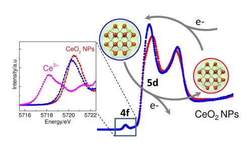
Time dependent cerium high energy resolution fluorescence detection X-ray adsorption spectroscopy (HERFD-XAS) of 3nm cerium dioxide particles before any chemical reaction (red curve) and during the catalase mimetic activity (bleu curve).A new chapter has been opened in our understanding of the chemical activity of nanoparticles says a team of international scientists. Using the X-ray beams of The European Synchrotron (ESRF) they showed that the electrons absorbed and released by cerium dioxide nanoparticles during chemical reactions behave in a completely different way than previously thought: the electrons are not bound to individual atoms but, like a cloud, distribute themselves over the whole nanoparticle. Inspired by the similarity of its shape, the scientists call this spatial distribution of particles an "electron sponge". The results were published on 12 November in the journal ACS Nano.


Today, cerium dioxide nanoparticles are widely used in industrial processes and also in consumer products. They are present, for example, in the walls of self-cleaning ovens and act as a hydrocarbon catalyst during the high temperature cleaning process. They are also a hot candidate for the next generation of lithium-ion batteries which will exhibit higher voltages and a greater storage capacity compared to today’s energy cells.

The element Cerium is abundant in the Earth’s crust and can easily be mined and purified. However, without a thorough understanding of the chemical processes that take place on the surface of cerium dioxide nanoparticles, it is impossible to optimise their current and future use. And to address a more complex issue, it is also impossible to assess the limits of their safe use.


TEM image.jpg
Transmission Electron Microscope (TEM) image of the 3nm CeO2 NPs
Most chemical reactions involve the transfer of an electron from one atom to another. In the past, it was believed that the electrons involved in a chemical reaction on the surface of a nanoparticle were localised in one of the atoms at the surface. To determine the behaviour of the electrons during the reaction, the scientists used the intense X-ray beams at the ESRF to probe solutions of nanoparticles in water and ethanol. The nanoparticles had a diameter of 3 nm and consisted of several thousands of molecules of cerium dioxide.
It is known that nanoparticles can change their behaviour under vacuum when studied with an electron microscope, for example. The scientists therefore carried out their experiment under realistic conditions, studying the nanoparticles in solution and in real time as the chemical reaction was taking place. “It was only possible to conduct these experiments in a liquid rather than under vacuum because we used X-rays as probes for the electron distribution." says Jean Daniel Cafun.

X-rays reveal an unexpected property of widely used nanoparticles


In their experiment, the scientists were successful in observing the creation of the nanoparticles in solution and then how these nanoparticles eliminated highly reactive molecules (reactive oxygen species, or ROS) from the solution. This elimination process mimics the role of an important enzyme in living organisms - catalase - that protects cells from these aggressive molecules. Cancer patients undergoing radiation therapy have high levels of ROS in their bodies and ceria nanoparticles have been proposed as a way of reducing the levels of ROS and thus alleviating the negative impacts of the therapy on the patients. Throughout the chemical reaction, the electronic structure of the cerium atoms and thus the redistribution of the electron cloud was monitored. "It is crucial to be able to study the chemical processes of the particles in an environment that is close to conditions found in biological systems.” emphasizes Victor Puntes.
HERFD-XAS cerium dioxide_resize.jpg
Time dependent cerium high energy resolution fluorescence detection X-ray adsorption spectroscopy (HERFD-XAS) of 3nm cerium dioxide particles before any chemical reaction (red curve) and during the catalase mimetic activity (bleu curve). The enlargement of the pre-edge spectra shows that during the catalytic reaction, all Ce ions remain electron-paired in CeO2 nano particles. The redox partner is therefore not a local, spin-unpaired Ce3+ site as has been generally assumed, but the electron density that is received and released during the catalytic reaction, is delocalized over the atoms of the nanoparticle. This invokes the picture of an electron sponge as shown in the cartoon diagram. The green surface represents the electron density distribution that expands or contracts when receiving or releasing electrons.
"Scientists have been discussing the question: What happens when electrons are added to ceria nanoparticles? The work by Cafun et al. is a key study because it questions the present, widely accepted model and will lead the research in a new direction," says Frank de Groot, an expert on nanomaterials at Utrecht University who did not take part in the experiment.

The next step, which has already been initiated, will be to assess whether non-localised electrons are a property of cerium dioxide only or also of other widely used nanoparticles like titanium dioxide. “In parallel, chemists have to revisit their theoretical models to explain the chemical behaviour of nanoparticles and to better understand how electrons are transferred in chemical reactions taking place on their surface,” concludes Pieter Glatzel.

Reference:
Jean-Daniel Cafun et al., Absence of Ce3+ Sites in Chemically Active Colloidal Ceria Nanoparticles, ACS Nano 12 November 2013, DOI:10.1021/nn403542p

Saturday, September 28, 2013

Researchers Demonstrate 'Accelerator on a Chip'


Technology could spawn new generations of smaller, less expensive devices for science, medicine

In an advance that could dramatically shrink particle accelerators for science and medicine, researchers used a laser to accelerate electrons at a rate 10 times higher than conventional technology in a nanostructured glass chip smaller than a grain of rice.

The achievement was reported today in Nature by a team including scientists from the U.S. Department of Energy’s (DOE) SLAC National Accelerator Laboratory and Stanford University.

“We still have a number of challenges before this technology becomes practical for real-world use, but eventually it would substantially reduce the size and cost of future high-energy particle colliders for exploring the world of fundamental particles and forces,” said Joel England, the SLAC physicist who led the experiments. “It could also help enable compact accelerators and X-ray devices for security scanning, medical therapy and imaging, and research in biology and materials science.”

Because it employs commercial lasers and low-cost, mass-production techniques, the researchers believe it will set the stage for new generations of "tabletop" accelerators.

At its full potential, the new “accelerator on a chip” could match the accelerating power of SLAC’s 2-mile-long linear accelerator in just 100 feet, and deliver a million more electron pulses per second.

This initial demonstration achieved an acceleration gradient, or amount of energy gained per length, of 300 million electronvolts per meter. That's roughly 10 times the acceleration provided by the current SLAC linear accelerator.

“Our ultimate goal for this structure is 1 billion electronvolts per meter, and we’re already one-third of the way in our first experiment,” said Stanford Professor Robert Byer, the principal investigator for this research.


How It Works


Today’s accelerators use microwaves to boost the energy of electrons. Researchers have been looking for more economical alternatives, and this new technique, which uses ultrafast lasers to drive the accelerator, is a leading candidate.

Particles are generally accelerated in two stages. First they are boosted to nearly the speed of light. Then any additional acceleration increases their energy, but not their speed; this is the challenging part.

In the accelerator-on-a-chip experiments, electrons are first accelerated to near light-speed in a conventional accelerator. Then they are focused into a tiny, half-micron-high channel within a fused silica glass chip just half a millimeter long. The channel had been patterned with precisely spaced nanoscale ridges. Infrared laser light shining on the pattern generates electrical fields that interact with the electrons in the channel to boost their energy. (See the accompanying animation for more detail.)

Turning the accelerator on a chip into a full-fledged tabletop accelerator will require a more compact way to get the electrons up to speed before they enter the device.

A collaborating research group in Germany, led by Peter Hommelhoff at Friedrich Alexander Universityand the Max Planck Institute of Quantum Optics, has been looking for such a solution. Itsimultaneously reports in Physical Review Letters its success in using a laser to accelerate lower-energy electrons.
Multi-Use Accelerators

Applications for these new particle accelerators would go well beyond particle physics research. Byer said laser accelerators could drive compact X-ray free-electron lasers, comparable to SLAC’s Linac Coherent Light Source, that are all-purpose tools for a wide range of research.

Another possible application is small, portable X-ray sources to improve medical care for people injured in combat, as well as provide more affordable medical imaging for hospitals and laboratories. That’s one of the goals of the Defense Advanced Research Projects Agency’s (DARPA) Advanced X-Ray Integrated Sources (AXiS) program, which partially funded this research. Primary funding for this research is from the DOE’s Office of Science.

The study's lead authors were Stanford graduate students Edgar Peralta and Ken Soong. Peralta created the patterned fused silica chips in the Stanford Nanofabrication Facility. Soong implemented the high-precision laser optics for the experiment at SLAC’s Next Linear Collider Test Accelerator. Additional contributors included researchers from the University of California-Los Angeles and Tech-X Corp. in Boulder, Colo.

SLAC is a multi-program laboratory exploring frontier questions in photon science, astrophysics, particle physics and accelerator research. Located in Menlo Park, California, SLAC is operated by Stanford University for the U.S. Department of Energy Office of Science. To learn more, please visitwww.slac.stanford.edu.

DOE’s Office of Science is the single largest supporter of basic research in the physical sciences in the United States, and is working to address some of the most pressing challenges of our time. For more information, please visit science.energy.gov.

Source: http://www6.slac.stanford.edu/news/2013-09-27-accelerator-on-a-chip.aspx